

A combined array element precise alignment assembly device and method
An assembly device and assembly method technology, which is applied in the direction of auxiliary devices, electrical components assembly of printed circuits, metal processing equipment, etc., can solve the problem that the position accuracy of the inner conductor is difficult to control, the quality of solder joints is difficult to guarantee, and the solder joints are prone to force, etc. problems, achieve good assembly quality, reliable quality, and ensure the effect of solder joint strength
- Summary
- Abstract
- Description
- Claims
- Application Information
AI Technical Summary
Problems solved by technology
Method used
Image

Examples
Embodiment Construction
[0045] In order to make the object, technical solution and advantages of the present invention clearer, the present invention will be further described in detail below in conjunction with the accompanying drawings and embodiments. It should be understood that the specific embodiments described here are only used to explain the present invention, not to limit the present invention. In addition, the technical features involved in the various embodiments of the present invention described below can be combined with each other as long as they do not constitute a conflict with each other. The present invention will be further described in detail below in combination with specific embodiments.
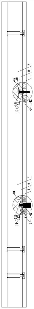
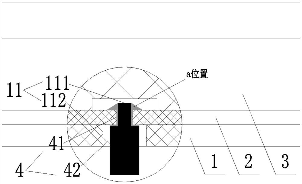
[0046] As a preferred embodiment of the present invention, such as Figure 1-9 As shown, the present invention provides a combined array element precise alignment assembly device, wherein:
[0047] The combined array element includes four-layer printed boards and five inner conductors;
...
PUM
 Abstract
Description
Claims
Application Information