Semiconductor device

A technology for semiconductors and conductive parts, which is applied in the fields of semiconductor devices, semiconductor/solid-state device components, and electric solid-state devices, etc., and can solve problems such as the degradation of the quality of semiconductor devices

Pending Publication Date: 2021-03-23
KK TOSHIBA +1
View PDF0 Cites 0 Cited by
  • Summary
  • Abstract
  • Description
  • Claims
  • Application Information

AI Technical Summary

Problems solved by technology

[0003] For example, depending on the condition of the conductive adhesive that connects the lead frame and connector together, the quality of such a semiconductor device may degrade

Method used


Image

  • Semiconductor device
  • Semiconductor device
  • Semiconductor device

Examples


no. 1 approach

[0015] Refer below Figure 1 to Figure 6 The first embodiment will be described. In this specification, components according to the embodiments and descriptions of these components can be described by various expressions. These components and their descriptions are exemplary and not limited by the expressions of this specification. Components may be identified by different nomenclature from those in this specification. These components may be described by expressions different from the expressions in this specification.

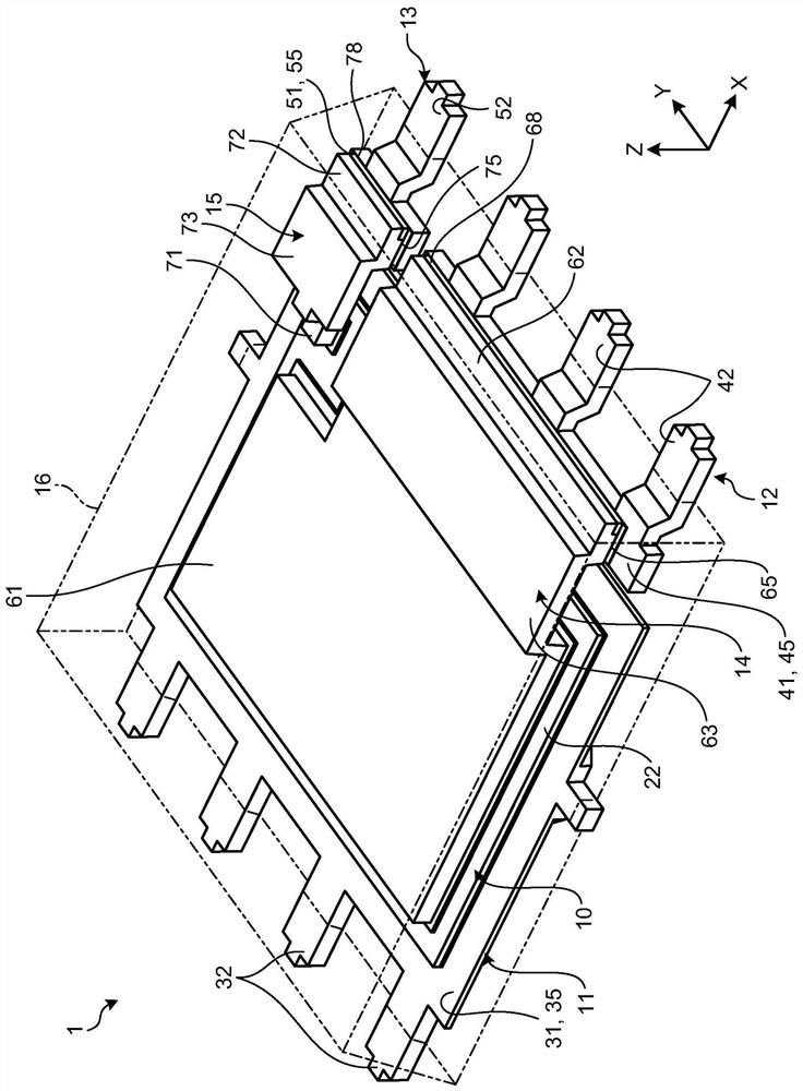
[0016] figure 1 is an exemplary perspective view of the semiconductor device 1 of the first embodiment. The semiconductor device 1 is, for example, a power device. The semiconductor device 1 is not limited to this example, and may be another device.

[0017] As shown in the drawings, in this specification, an X-axis, a Y-axis, and a Z-axis are defined for convenience. The X-axis, Y-axis and Z-axis are orthogonal to each other. The X-axis is set along ...

no. 2 approach

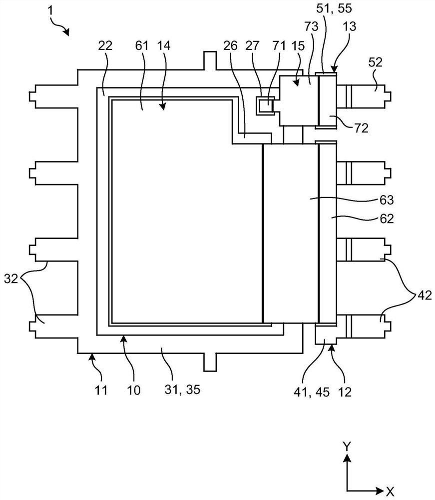
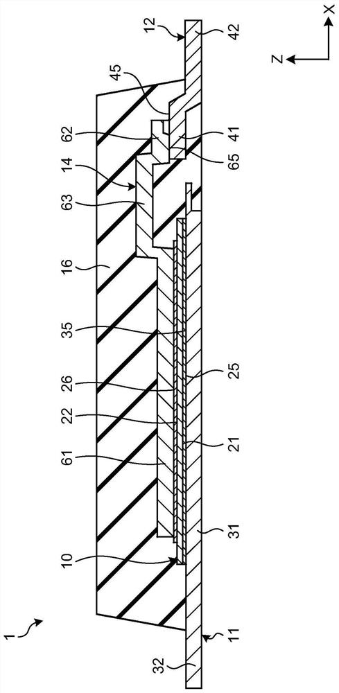
[0099] Refer below Figure 7 to Figure 9 The second embodiment will be described. In the description of the following embodiments, components having functions similar to those of components already described are denoted by the same reference numerals as components already described, and descriptions thereof may be omitted. A plurality of components denoted by the same symbol are not necessarily common for all functions and characteristics, and may have different functions and characteristics according to various embodiments.

[0100] Figure 7 is an exemplary schematic perspective view of a part of the second lead frame 12 and the first connector 14 according to the second embodiment. Figure 8 is a schematic sectional view of a part of the second lead frame 12 and the first connector 14 of the second embodiment. Figure 9 is an exemplary schematic plan view of the second connection surface 45 and the fourth connection surface 65 of the second embodiment.

[0101] like F...


PUM


Abstract

A semiconductor device according to one embodiment includes a first leadframe, a second leadframe, a semiconductor chip, and a conductive member. The second leadframe has a first face provided with arecess and is separated from the first leadframe. The semiconductor chip is mounted on the first leadframe. The conductive member has a second face connected to the first face with a conductive adhesive, the second face provided with a protrusion housed in the recess at least partially, and the conductive member electrically connected the semiconductor chip and the second leadframe to each other.The recess and the protrusion are longer in a first direction in which the first face extends than in a second direction along the first face and orthogonal to the first direction.

Description

technical field [0001] In general terms, the embodiments described herein relate to semiconductor devices. Background technique [0002] A known semiconductor device includes a lead frame and a semiconductor chip having electrodes, wherein the lead frame and the electrodes are electrically connected to each other, for example, by a board-like connector. The electrodes and the connector, and the lead frame and the connector are mechanically and electrically connected to each other through a conductive adhesive such as solder. [0003] For example, depending on the condition of the conductive adhesive that connects the lead frame and the connector together, the quality of such a semiconductor device may degrade. Contents of the invention [0004] According to one embodiment, a semiconductor device includes a first lead frame, a second lead frame, a semiconductor chip, and a conductive member. The second lead frame is spaced apart from the first lead frame and has a first f...

Claims


Application Information

Patent Timeline
IPC IPC(8): H01L23/495
CPCH01L23/49537H01L23/49562H01L23/49551H01L23/49524H01L23/49548H01L2224/4103H01L2224/40245H01L2224/0603H01L2924/181H01L2224/32245H01L2224/40095H01L2924/00012
Inventor 山口翔唐泽纯
Owner KK TOSHIBA
Why Eureka
Try Eureka