Optical device test fixture and test device thereof

A technology for testing fixtures and optical devices, which is applied in the field of optical communications and can solve the problems of pins and circuit boards exposed to high temperature and high humidity environments

Pending Publication Date: 2021-03-26
GUANGXUN SCI & TECH WUHAN +1
View PDF0 Cites 0 Cited by
  • Summary
  • Abstract
  • Description
  • Claims
  • Application Information

AI Technical Summary

Problems solved by technology

[0004] In view of this, the embodiment of the present application expects to provide a test fixture and a test device for an optical device to solve the problem that the pins and circuit boards of the optical device are directly exposed to high temperature and high humidity during the aging process

Method used


Image

  • Optical device test fixture and test device thereof
  • Optical device test fixture and test device thereof
  • Optical device test fixture and test device thereof

Examples


Embodiment Construction

[0044] It should be noted that in the case of an unable conflict, the technical features in the present application and the technical features in the embodiments can be combined, and the detailed description in the specific embodiments should be understood as explanation purposes of the present application, should not be considered Improper limitation of the present application.

[0045] The orientation terminology in the description of the present application is mean to facilitate the description of the present application and simplification, rather than indicating or implying that the device or element must have a specific orientation, and therefore cannot be understood as a specific orientation. limits.

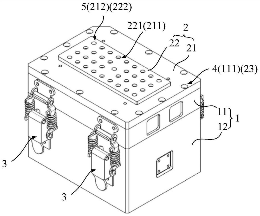
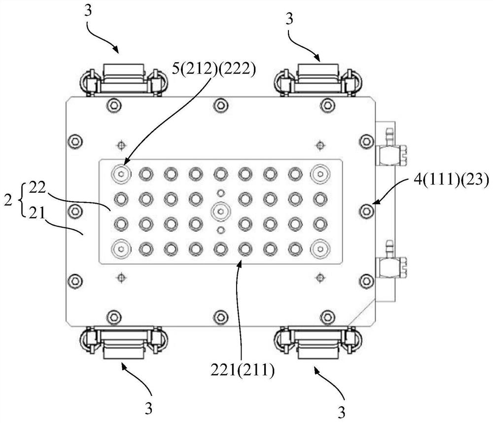
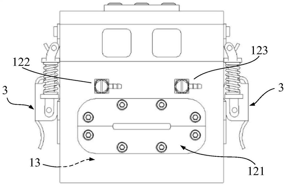
[0046] In the field of optical communications, traditional optical components are generally in a hermetically packaged form because the chips such as the conventional laser or detectors are not directly placed in a non-controlled environment. The problem of airtight package is...


PUM


Abstract

The invention provides a test fixture of an optical device and a test device thereof. The test fixture comprises a box body, a clamping assembly and a circuit board. The box body is provided with an accommodating cavity capable of sealing protective gas and a flat cable interface, and the clamping assembly is arranged on the box body and used for clamping an optical device. The circuit board is arranged in the containing cavity, pins of the optical device are connected with the circuit board, and the circuit board is electrically connected with the outside through the flat cable interface. According to the test fixture of the optical device and the test device thereof provided by the invention, the tube cap and the circuit board of the optical device are arranged in the accommodating cavity, so the optical device is prevented from being directly exposed in a high-temperature and high-humidity environment, and the tube cap and the circuit board are effectively protected.

Description

Technical field [0001] The present application relates to the field of optical communication, and more particularly to a light device test fixture and a test device thereof. Background technique [0002] For optical devices, such as TO-CAN (Transistor Outline CAN, cohaxing laser diode module), as required to have a certain high temperature under the conditions of charged constant humidity, High humidity tolerance, therefore requires charging agents of the chip under high temperature and high humidity. [0003] In the prior art, when charging the chip, the optical device is typically clamped through the test device and power it. In the process of aging, the circuit board and the pin of the circuit board and the pin in the test device are usually exposed directly to the high-temperature and high humidity environment, thereby causing the performance of the components such as the circuit board and the optical device. Impact. Inventive content [0004] In view of this, the present ap...

Claims


Application Information

Patent Timeline
IPC IPC(8): G01R1/04G01R31/00
CPCG01R1/0425G01R31/003
Inventor 陈玲玲曾笔鉴熊永华余洁万枫陈佳俊白山大地
Owner GUANGXUN SCI & TECH WUHAN
Why Eureka
Try Eureka