A method for fabricating an oxidation-enhanced diode

A manufacturing method and diode technology, applied to semiconductor devices, electrical components, circuits, etc., can solve the problems of multiple cycles, multiple product classifications, uneven oxidation, etc., and achieve the effects of improving product performance, reducing costs, and reducing process time

Active Publication Date: 2022-02-25
XIAN LIXIN PHOTOELECTRIC SCI & TECH
View PDF11 Cites 0 Cited by
  • Summary
  • Abstract
  • Description
  • Claims
  • Application Information

AI Technical Summary

Problems solved by technology

[0003] The purpose of the present invention is to solve the problems of uneven oxidation, high series resistance, many product classifications and more cycles in the existing diode production method, and provide a production method of oxidation-enhanced diode

Method used


Image

  • A method for fabricating an oxidation-enhanced diode
  • A method for fabricating an oxidation-enhanced diode
  • A method for fabricating an oxidation-enhanced diode

Examples


Embodiment Construction

[0032] The content of the present invention will be further described in detail below in conjunction with the accompanying drawings and specific embodiments.

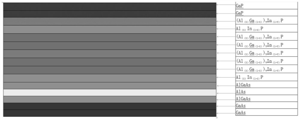
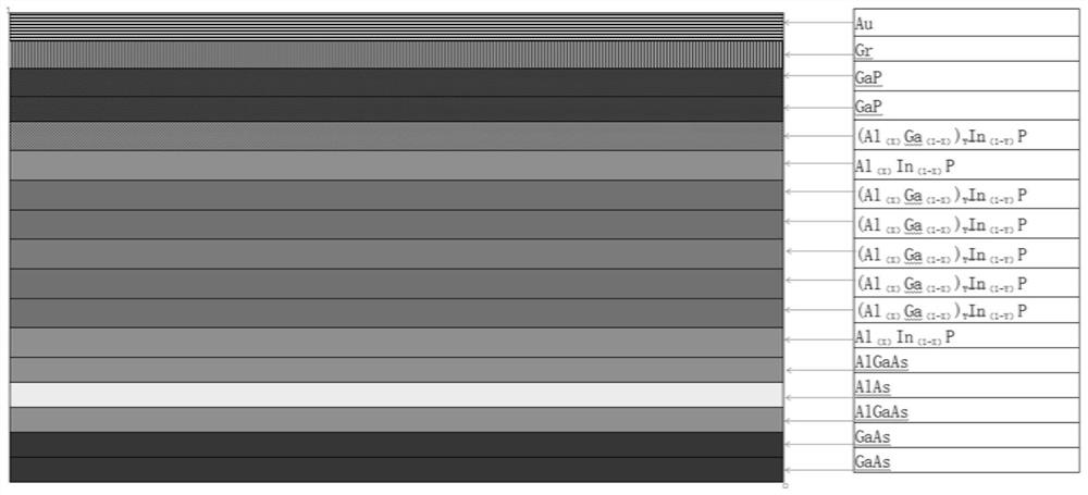
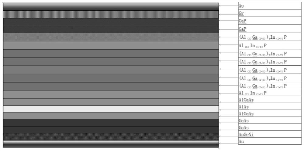
[0033] The invention provides a method for making an oxidation-increased diode. When the method of the invention is growing AlAs, 40-100PPM of O (oxygen) element is added to TMAl, so that the oxidation uniformity of the product is improved. Decrease from 3.09 to 1.77, increase ΔN, improve device performance.

[0034] The method for making an oxidation-enhanced diode provided by the present invention comprises the following steps:

[0035] Step 1. Use epitaxial MOCVD equipment to grow an epitaxial structure on a GaAs substrate. The growth components of the structure are grown sequentially from bottom to top. The growth temperature is 550-700°C, the growth pressure is 40-50 torr, and the preferred pressure is 42 torr. When growing, add 40-100PPM O (oxygen) element in TMAl;

[0036] Step 2, making the front metal electro...


PUM

PropertyMeasurementUnit
refractive indexaaaaaaaaaa

Abstract

The invention provides a method for manufacturing an oxidation-increased diode, which solves the problems of uneven oxidation, high series resistance, many product classifications, and many cycle times in the existing diode manufacturing method. The method includes: step 1, growing an epitaxial structure on a GaAs substrate, adding 40-100PPM oxygen element in TMAl during AlAs growth; step 2, making a front metal electrode; step 3, making a back metal; step 4, Graphic production; step five, annealing at 350-450°C in a protective gas environment; step six, cutting; step seven, AlAs oxidation, oxidation gas conditions: increase water vapor in a protective gas environment, and the outlet temperature of the mixed gas is 90 ~100°C; step 8, perform chip test. In the method of the present invention, a small amount of oxygen element is added in TMAl, so that the oxidation uniformity of the product is improved, and at the same time, AlAs is oxidized and becomes Al 2 o 3 , The refractive index is reduced from 3.09 to 1.77, increasing ΔN and improving the performance of the device.

Description

technical field [0001] The invention relates to the field of diode manufacture, in particular to a method for manufacturing an oxidation enhanced diode. Background technique [0002] Due to the advantages of low power consumption, small size and high reliability, light-emitting diodes have been developed rapidly as the main light source. In recent years, light-emitting diodes have rapidly expanded in the field of lighting applications, and are developing towards higher luminous power. In the prior art, a multiple quantum well (multiple quantum well, MQW) structure is used as the light-emitting diode of the active layer, and this structure can obtain a higher internal quantum efficiency, while the improvement of the external quantum efficiency of the light-emitting diode mainly focuses on surface roughening, Metal mirror technology, graphic substrates, etc. However, the existing oxidation-intensifying diode manufacturing method has disadvantages such as uneven oxidation, hi...

Claims


Application Information

Patent Timeline
Patent Type & Authority Patents(China)
IPC IPC(8): H01L33/32H01L33/36H01L33/40H01L33/44H01L33/26H01L33/00
CPCH01L33/32H01L33/26H01L33/0075H01L33/44H01L33/36H01L33/40
Inventor 夏黎明李青民任占强李喜荣王宝超张超奇孙丞李波
Owner XIAN LIXIN PHOTOELECTRIC SCI & TECH
Why Eureka
Try Eureka