
In-situ surface shape splicing measurement device and method for large-aperture planar optical element

A technology of optical components and measuring devices, applied in the field of optics, can solve problems such as being easily affected by air flow disturbance and vibration, low resolution of surface shape measurement, and inability to measure

Active Publication Date: 2021-03-30
XI'AN INST OF OPTICS & FINE MECHANICS - CHINESE ACAD OF SCI
View PDF6 Cites 5 Cited by
  • Summary
  • Abstract
  • Description
  • Claims
  • Application Information

AI Technical Summary

Problems solved by technology

[0006] In order to solve the problem that the existing schemes for measuring the surface shape of large-aperture planar optical elements are easily affected by air flow disturbance and vibration, the measurement dynamic range is small, the resolution of surface shape measurement is not high, and it cannot be applied to various attitude and surface shape measurements in situ. As well as the technical problem that it cannot be measured when there is Power in the surface shape of the large-diameter plane optical element, the present invention proposes a large-diameter plane optical element splicing measurement device and method, which can realize the large-diameter plane optical element in-situ Dynamic and high-precision measurement of surface shape under various attitudes, especially the in-position surface shape measurement of planar optical elements with large power, and the measurement accuracy is not affected by the external environment (air flow disturbance, vibration, etc.)

Method used


Image

  • In-situ surface shape splicing measurement device and method for large-aperture planar optical element
  • In-situ surface shape splicing measurement device and method for large-aperture planar optical element
  • In-situ surface shape splicing measurement device and method for large-aperture planar optical element

Examples


Embodiment Construction

[0074] The present invention will be further described below in conjunction with accompanying drawing.

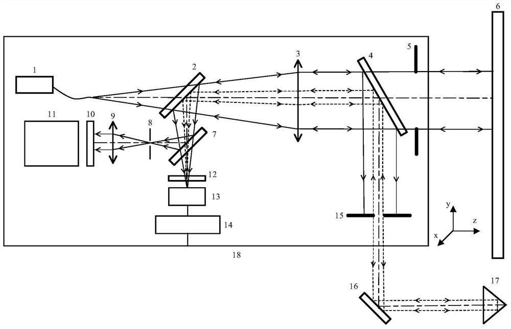
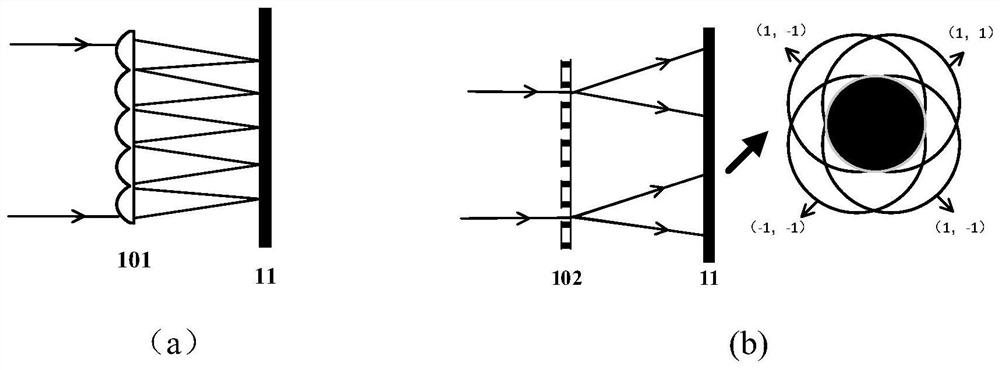
[0075] Such as figure 1 As shown, the large-aperture planar optical element provided by the present invention is an in-plane shape splicing measurement device, including an image data processing unit (not shown in the figure), a six-degree-of-freedom motion platform 18, and a six-degree-of-freedom motion platform 18 The laser 1, the first half mirror 2, the collimating objective lens 3, the second half mirror 4, the diaphragm 5, the third half mirror 7, the aperture diaphragm 8 with an aperture less than 1mm, Collimating eyepiece 9 , binary optical device 10 , detector 11 , attenuation plate 12 , far-field detector 13 , drive controller 14 , electric control diaphragm 15 , mirror array 16 and corner cube array 17 .

[0076] The first half-mirror 2, the collimating objective lens 3, the second half-mirror 4, the diaphragm 5 and the measured large-aperture planar optical ele...


PUM


Abstract

In order to solve the technical problems that the existing scheme for measuring the surface shape of the large-aperture planar optical element is easily influenced by air flow disturbance and vibration, the measurement dynamic range is small, the surface shape measurement resolution is not high, the scheme cannot be applied to surface shape measurement of various postures in place, and measurementcannot be performed when Power exists in the surface shape of the large-aperture planar optical element, the invention provides an in-situ surface shape splicing measurement device and method for a large-aperture plane optical element. A laser, a semi-transparent semi-reflective mirror, a collimator objective, a diaphragm, a small-hole diaphragm, a collimator eyepiece, a binary optical device, adetector, an attenuation plate, a far-field detector, a drive controller, an electric control diaphragm, a reflector array, a pyramid prism array and a six-degree-of-freedom motion platform are utilized, the dynamic high-precision surface shape splicing measurement of the measured large-aperture planar optical element under various postures is realized, and the measurement precision is not influenced by the external environment.

Description

technical field [0001] The invention belongs to the field of optics, and relates to a large-caliber plane optical element surface shape measuring device and a method thereof. The large-aperture planar optical element mentioned in the present invention refers to a planar optical element with an aperture larger than 300 mm. Background technique [0002] Large-aperture planar optical components are mainly used in astronomical telescopes, high-power laser inertial confinement fusion and other devices. Since the large-aperture planar optical element is in a tilted working posture, the surface shape will be affected by factors such as gravity, supporting fixtures, and adjustment status, and will be deformed, which will seriously affect the stability of the device and the wavefront quality of the output beam. Therefore, it is of great significance to realize the measurement of the in-situ surface shape of large-aperture planar optical elements, and adjust the posture or support fi...

Claims


Application Information

Patent Timeline
IPC IPC(8): G01B11/24G06F17/14G06T7/62G06T7/66G06T7/73G06T17/20
CPCG01B11/2441G06F17/142G06T17/20G06T7/62G06T7/66G06T7/73
Inventor 段亚轩达争尚陈晓义袁索超范尧李铭王璞
Owner XI'AN INST OF OPTICS & FINE MECHANICS - CHINESE ACAD OF SCI
Learn More