Testability design method for embedded IP of FPGA

A design method and testing technology, applied in CAD circuit design, special data processing applications, etc., can solve problems such as the reduction of DFT coverage, and achieve the effect of improving DFT test coverage

Active Publication Date: 2021-04-02
SHENZHEN PANGO MICROSYST CO LTD
View PDF3 Cites 3 Cited by
  • Summary
  • Abstract
  • Description
  • Claims
  • Application Information

AI Technical Summary

Problems solved by technology

[0004] In the prior art, IP configuration points or control information are sampled through registers after entering the IP through a series of combinatorial logics. This part of the combinatorial logic cannot achieve DFT test coverage by inserting register chains (the aforementioned sampled registers), thus Resulting in reduced DFT coverage for IP

Method used


Image

  • Testability design method for embedded IP of FPGA
  • Testability design method for embedded IP of FPGA
  • Testability design method for embedded IP of FPGA

Examples


Embodiment Construction

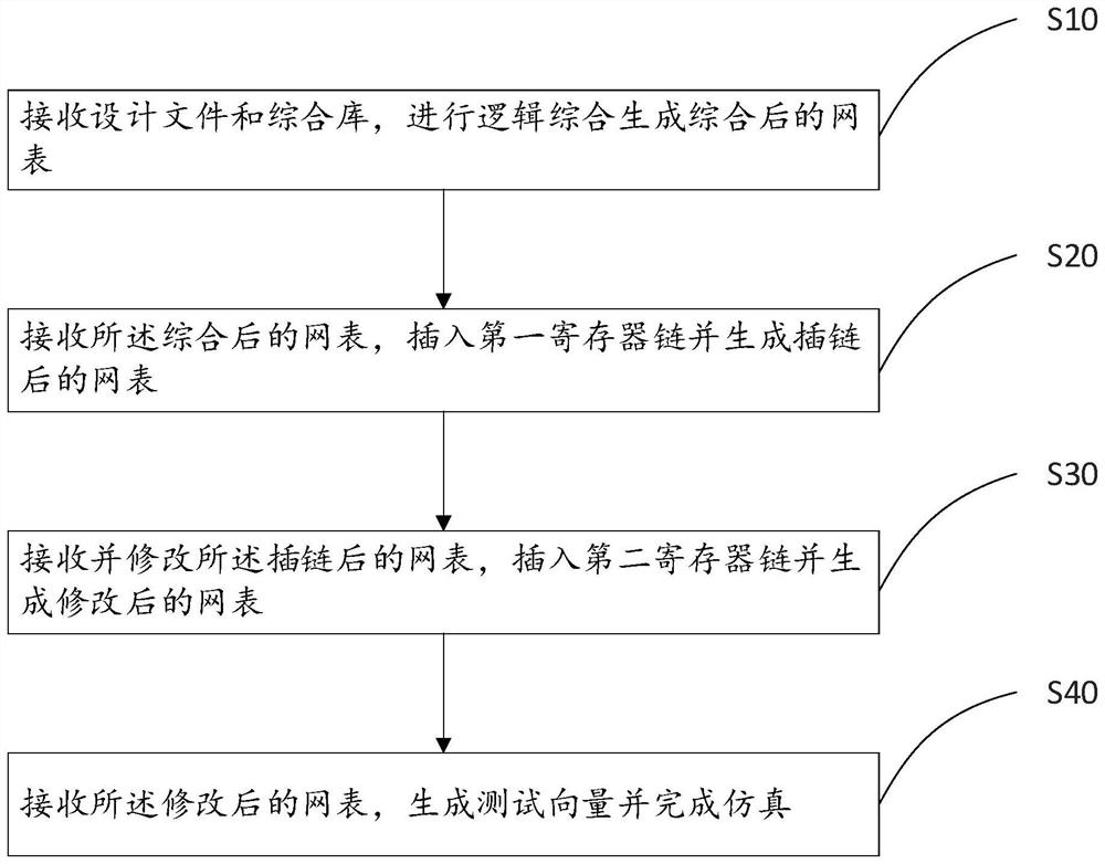
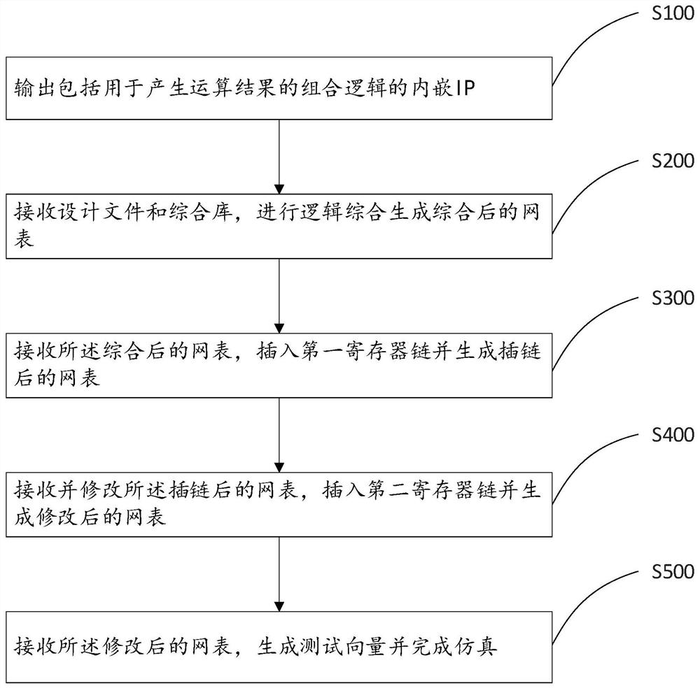
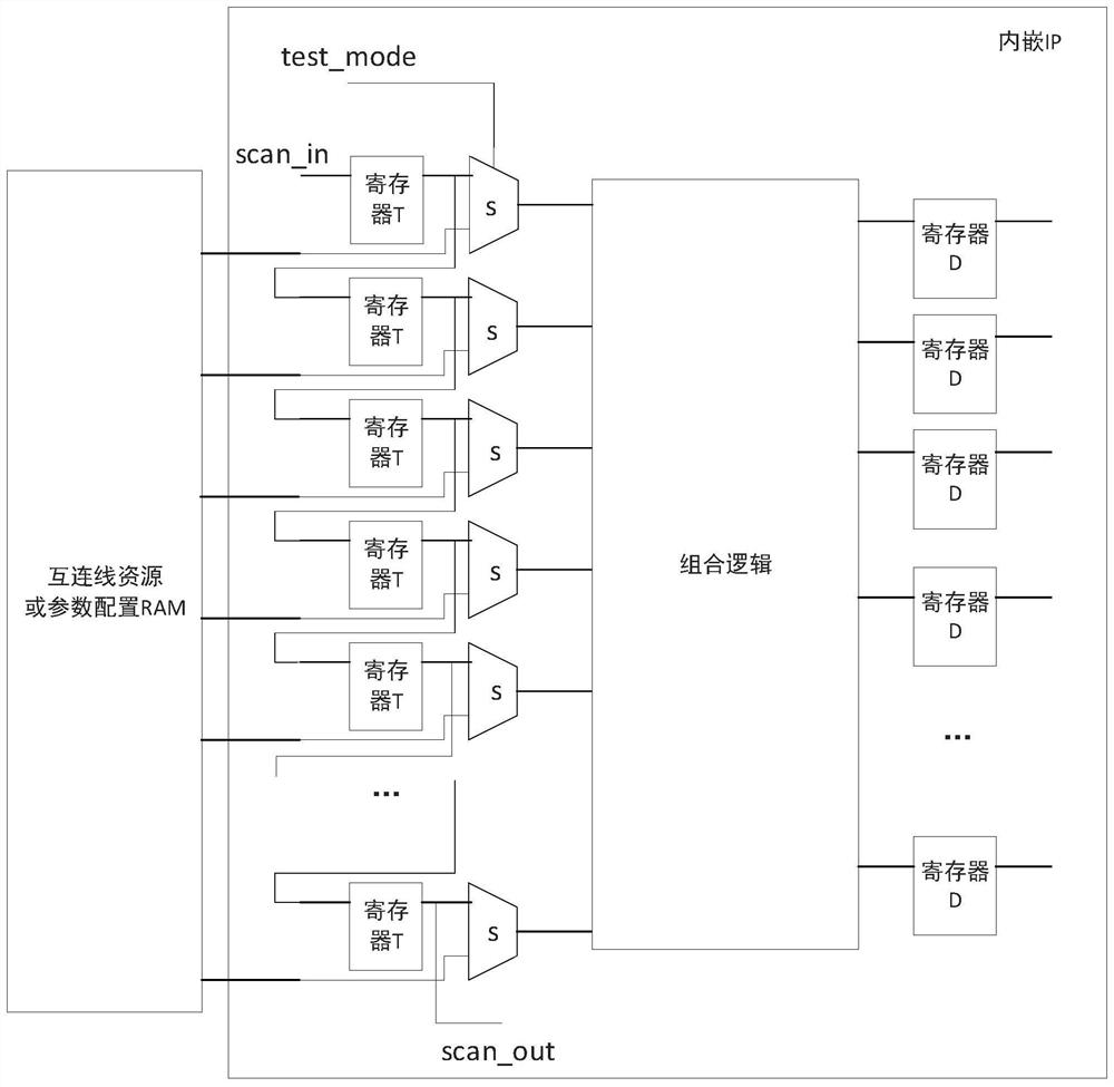
[0020]In order to make this specification, the technical solutions and advantages will be described in conjunction with the specific embodiments and corresponding drawings of the present specification and the corresponding drawings. Obviously, the described embodiments are merely the embodiments of the present specification, not all of the embodiments. Based on the embodiments in this specification, one of ordinary skill in the art does not have all other embodiments obtained without creative labor, all of which are protected by this specification. It should be noted that the features in the embodiments and embodiments in the present application may be combined with each other in the case of an unable conflict.

[0021]The description and claims of the invention and the terms "first", "second" and "third", and the like in the above drawings are for distinguishing different objects rather than to describe a particular order. Moreover, the terms "include" and any variation, intending to ...


PUM


Abstract

The invention provides a testability design method for an embedded IP of an FPGA, and the method comprises the steps: receiving a design file and a comprehensive library, and carrying out the logic synthesis to generate a synthesized netlist; receiving the integrated netlist, inserting a first register chain and generating a chain-inserted netlist; receiving and modifying the chain-inserted netlist, inserting a second register chain and generating a modified netlist; and receiving the modified netlist, generating a test vector and completing simulation. According to the testability design method, the input excitation of the embedded IP is changed by inserting the second register chain, so that the defects in the embedded IP can be detected through a DFT case; and the DFT test coverage rateof the embedded IP can be obviously improved on the premise that the circuit structure of the embedded IP is prevented from being greatly modified.

Description

[Technical field][0001]The present invention relates to the field of integrated circuit chips, and more particularly to a testic design method for FPGA embedding IP.【Background technique】[0002]Testability Design (DFT, Design for Test) is a key link for larger-scale digital IC design. Before performing specific functional testing of the sample, the DFT test vector can quickly filter the sample with process defects, thereby greatly improved Sample test efficiency. Among them, the coverage of the test vector reflects that the DFT design can detect the probability of the sample defect, the higher the coverage, the better the sample inspection, the smaller the missing samples may be.[0003]Unlike the ASIC, the FPGA design includes both the programmable logic part of the custom circuit design, including logical integration, layout wiring, and the like by standard process libraries, layout, etc., such as PCIe controller. , DDR controller, etc. Therefore, the DFT design of the entire chip ca...

Claims


Application Information

Patent Timeline
Patent Type & Authority Applications(China)
IPC IPC(8): G06F30/33
CPCG06F30/33
Inventor 季顺南张勇王俊温长清
Owner SHENZHEN PANGO MICROSYST CO LTD
Why Eureka
Try Eureka