Wafer position detection device

A detection device and wafer technology, which is applied in the manufacturing of electrical components, circuits, semiconductor/solid-state devices, etc., can solve the problems of limited application scope of sensors, impact on yield, sensor defects, etc., to reduce the scratch area and improve the finished product. efficiency, and the effect of improving versatility

Active Publication Date: 2021-04-06
HANGZHOU ZHONGGUI ELECTRONICS TECH CO LTD
View PDF4 Cites 1 Cited by
  • Summary
  • Abstract
  • Description
  • Claims
  • Application Information

AI Technical Summary

Problems solved by technology

[0005] In view of this, the object of the present invention is to provide a wafer position detection device to solve the problem that the indirect detection sensor is easy to produce defects on the wafer surface, which affects the yield, and the direct detection sensor has limited application range.

Method used


Image

  • Wafer position detection device
  • Wafer position detection device
  • Wafer position detection device

Examples


Embodiment Construction

[0039] The embodiment of the present invention discloses a wafer position detection device, so as to solve the problem that the wafer surface is defective due to the direct contact of the sensor and affects the yield.

[0040] The technical solutions in the embodiments of the present invention will be clearly and completely described below with reference to the accompanying drawings in the embodiments of the present invention. Obviously, the described embodiments are only a part of the embodiments of the present invention, but not all of the embodiments. Based on the embodiments of the present invention, all other embodiments obtained by those of ordinary skill in the art without creative efforts shall fall within the protection scope of the present invention.

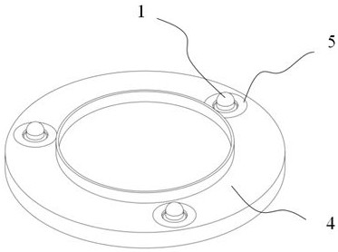
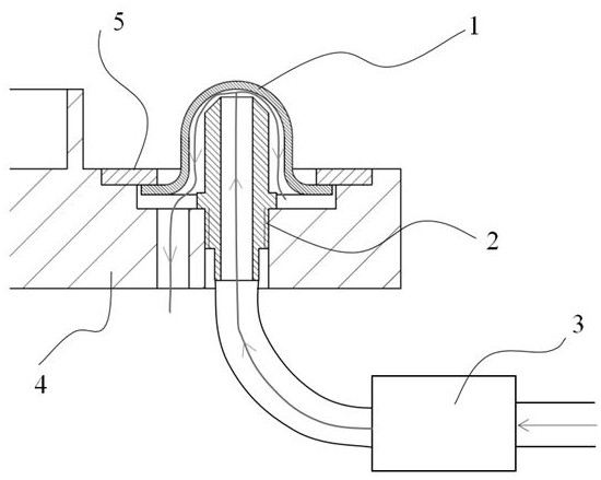
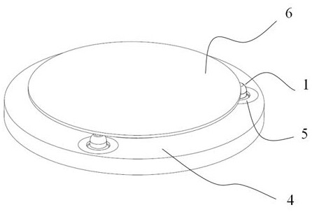
[0041] see Figure 1-Figure 7 , figure 1 A schematic diagram of the appearance structure of the wafer position detection device provided by the embodiment of the present invention; figure 2 for figure 1 Schematic d...


PUM


Abstract

The invention discloses a wafer position detection device. The wafer position detection device comprises a mounting base, a trigger assembly and a fluid pressure detection assembly, the trigger assembly arranged on the mounting base comprises a top cover protruding out of the surface of the mounting base to support the wafer and a fluid conveying pipeline arranged in a hollow cavity formed by the inner wall of the top cover, and when the wafer is arranged on the top cover, the top cover can move in the direction close to the fluid conveying pipeline to block a fluid conveying port of the fluid conveying pipeline; when no wafer is arranged on the top cover, the top cover can move in the direction away from the fluid conveying pipeline under the action of fluid pressure to conduct the fluid conveying port of the fluid conveying pipeline; the fluid pressure detection assembly is indirectly contacted with the wafer through the top cover to indirectly detect the in-place condition of the wafer, so that the problem that the yield is influenced due to defects generated on the surface of the wafer caused by direct contact is prevented; and compared with an optical sensor, in-place detection of wafers sensitive to illumination can be achieved, the application range is wide, and the universality of the device is improved.

Description

technical field [0001] The present invention relates to the field of semiconductor processing equipment, and more particularly, to a wafer position detection device. Background technique [0002] In recent years, with the rapid development of the semiconductor industry, the manufacturing process line width of semiconductor chips has been reduced from 0.18um to less than 10nm, and the number of metal layers has increased from 5-6 layers to more layers. The copper process multi-layer wiring solves the problem of aluminum interconnection The bottleneck problem of the process also puts forward higher requirements for the global flattening. CMP is currently the best global planarization technology and an essential process link in the copper interconnect process. Copper (Cu) CMP process is prone to corrosion defects in addition to butterfly, erosion, and scratches. [0003] Various parts of CMP planarization equipment require real-time detection of wafer position. For example, ...

Claims


Application Information

Patent Timeline
Patent Type & Authority Applications(China)
IPC IPC(8): H01L21/67
CPCH01L21/67265H01L21/67253H01L21/67017
Inventor 徐枭宇
Owner HANGZHOU ZHONGGUI ELECTRONICS TECH CO LTD
Why Eureka
Try Eureka