LED packaging structure and manufacturing method thereof

A technology of LED packaging and manufacturing methods, which is applied in the direction of electrical components, electrical solid devices, circuits, etc., can solve the problems of serious light absorption and low brightness of black glue, and achieve the effects of increasing brightness, improving contrast, and preventing cross-lighting

Pending Publication Date: 2021-04-09
APT ELECTRONICS
View PDF0 Cites 0 Cited by
  • Summary
  • Abstract
  • Description
  • Claims
  • Application Information

AI Technical Summary

Problems solved by technology

However, this packaging method has serious light absorption, resulting in low brightness of the LED.

Method used


Image

  • LED packaging structure and manufacturing method thereof
  • LED packaging structure and manufacturing method thereof
  • LED packaging structure and manufacturing method thereof

Examples


Embodiment 1

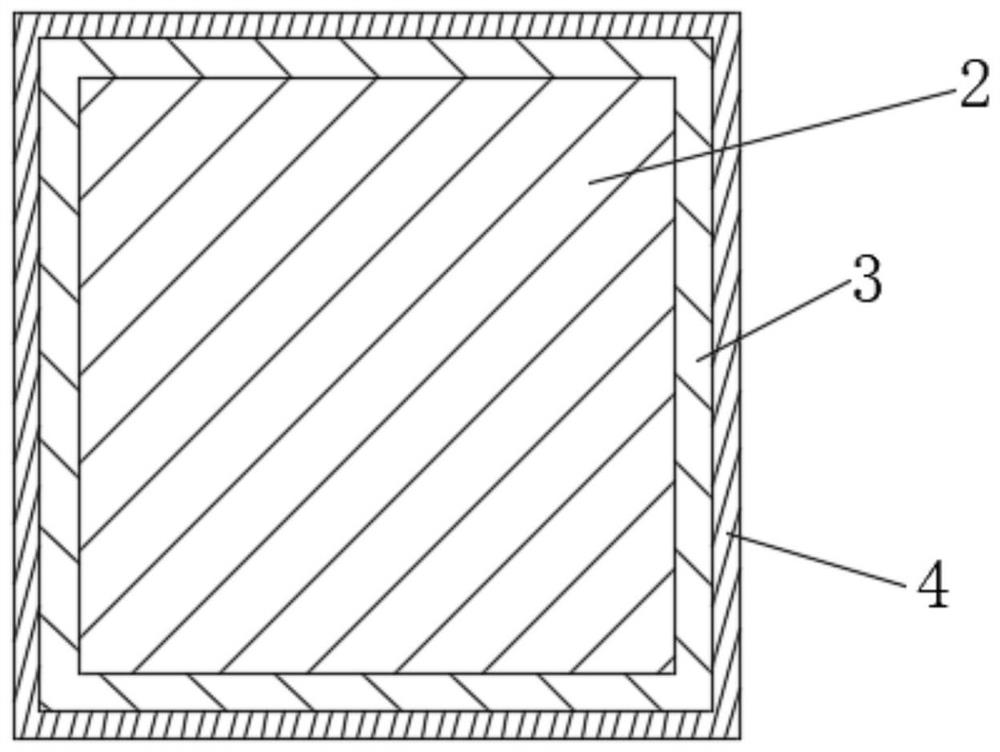
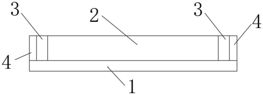
[0042] This embodiment provides a kind of LED encapsulation structure, refer to Figure 1-2 , including a substrate 1, an LED chip, a transparent adhesive layer 2, a white adhesive layer 3, and a black adhesive layer 4; the LED chip is an RGB chip.

[0043] The LED chip (not shown) is arranged on the substrate 1; the transparent adhesive layer 2 is laid on the substrate 1 and coated on the LED chip; the transparent adhesive layer 2 is used to diverge the light emitted by the LED chip to improve the light color uniformity of the LED properties; the white glue layer 3 is arranged around the transparent glue layer 2, and is used to reflect the light that is diverged to the white glue layer 3, avoiding a large amount of light being absorbed by the black glue layer 4, and improving the brightness of the LED; the black glue layer 4 Surrounded and arranged outside the white glue layer 3, the contrast can be improved, and the light emitted by other surrounding LED chips can be absorbe...

Embodiment 2

[0047] This embodiment provides a method for manufacturing the LED package structure as described in Embodiment 1, comprising the following steps:

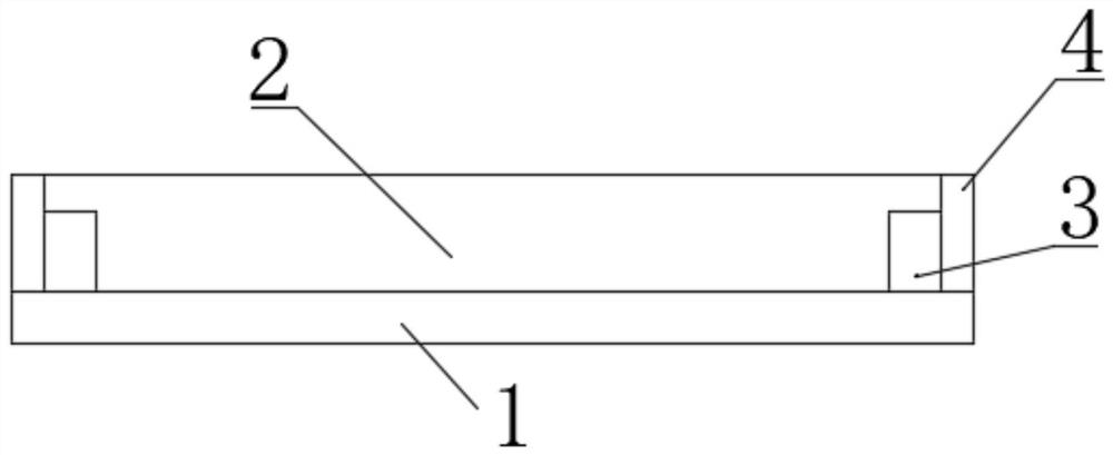
[0048] refer to Figure 4-6 , step S10, surround the first wall 5 around the edge of the substrate 1, the first wall 5 and the substrate 1 form a groove 6, add liquid transparent glue into the groove 6, and form a transparent glue after the liquid transparent glue is cured Layer 2;

[0049] Specifically, there are multiple LED chips (not shown) on the substrate 1; after the first wall 5 is set on the substrate 1, the first wall 5 forms a groove 6 with the substrate 1, and liquid transparent glue is added to form a transparent glue layer. 2.

[0050] In some embodiments, after the step of S10, it also includes

[0051] S11, polishing the surface of the transparent adhesive layer 2 to a preset target height.

[0052] refer to Figure 7 , S20, slotting the transparent adhesive layer 2, the surface of the transparent adhesive lay...


PUM

PropertyMeasurementUnit
Thicknessaaaaaaaaaa
Thicknessaaaaaaaaaa

Abstract

The invention discloses an LED packaging structure and a manufacturing method. The LED packaging structure comprises a substrate, an LED chip, a transparent adhesive layer, a white adhesive layer and a black adhesive layer. The LED chip is arranged on the substrate; the transparent adhesive layer is laid on the substrate and wraps the LED chip; the transparent adhesive layer is used for diffusing light emitted by the LED chip; the white adhesive layer is arranged outside the transparent glue layer in a surrounding manner and is used for reflecting light rays diffused to the white adhesive layer; the black adhesive layer is arranged outside the white adhesive layer in a surrounding mode and used for absorbing light emitted by other surrounding LED chips. According to the invention, the brightness of the LED packaged by the black adhesive can be increased.

Description

technical field [0001] The invention belongs to the field of photoelectric technology, and in particular relates to an LED packaging structure and a manufacturing method. Background technique [0002] The existing small-pitch LEDs are directly packaged with vinyl. Although this LED packaging method has a softer light output effect, it also improves the contrast. However, this packaging method has serious light absorption by vinyl, resulting in low brightness of the LED. Contents of the invention [0003] In order to overcome the above-mentioned shortcomings of the prior art, the purpose of the present invention is to provide an LED package structure and a manufacturing method, which can increase the brightness of the LED packaged in black glue. [0004] In the first aspect, the present invention provides an LED packaging structure, including a substrate, an LED chip, a transparent adhesive layer, a white adhesive layer, and a black adhesive layer; [0005] The LED chip i...

Claims


Application Information

Patent Timeline
IPC IPC(8): H01L25/075H01L33/52H01L33/56H01L33/60
CPCH01L25/0753H01L33/52H01L33/56H01L33/60
Inventor 林仕强万垂铭朱文敏徐波曾照明肖国伟
Owner APT ELECTRONICS
Why Eureka
Try Eureka