
Buried gate structure and fabrication method thereof

A manufacturing method and gate structure technology, applied in semiconductor/solid-state device manufacturing, semiconductor devices, electrical components, etc., can solve problems such as small drive current, increase gate current, increase discharge time, and solve drive The effect of small current

Active Publication Date: 2022-07-05
CHANGXIN MEMORY TECH INC
View PDF11 Cites 0 Cited by
  • Summary
  • Abstract
  • Description
  • Claims
  • Application Information

AI Technical Summary

Problems solved by technology

[0004] Based on this, in order to solve the problem of small driving current caused by inconsistent gate trench depths in semiconductor devices, a buried gate structure and its manufacturing method are provided.

Method used


Image

  • Buried gate structure and fabrication method thereof
  • Buried gate structure and fabrication method thereof
  • Buried gate structure and fabrication method thereof

Examples


Embodiment Construction

[0041] In order to make the above objects, features and advantages of the present invention more clearly understood, the specific embodiments of the present invention will be described in detail below with reference to the accompanying drawings. In the following description, numerous specific details are set forth in order to provide a thorough understanding of the present invention. However, the present invention can be implemented in many other ways different from those described herein, and those skilled in the art can make similar improvements without departing from the connotation of the present invention. Therefore, the present invention is not limited by the specific implementation disclosed below.

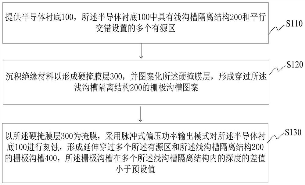
[0042] See image 3 and Figure 4 , an embodiment of the present invention provides a method for fabricating a buried gate structure, including:

[0043] In step S110, a semiconductor substrate 100 is provided, and the semiconductor substrate 100 has a shallow trench isol...


PUM

PropertyMeasurementUnit
percent by volumeaaaaaaaaaa

Abstract

The present invention relates to a buried gate structure and a manufacturing method thereof. The method for fabricating a buried gate comprises: providing a semiconductor substrate with a shallow trench isolation structure and a plurality of active regions arranged in parallel and staggered; forming and patterning a hard mask layer to form a Gate trench pattern; using the hard mask layer as a mask, the semiconductor substrate is etched using a pulsed bias power output mode to form gate trenches extending through multiple active regions and shallow trench isolation structures The difference between the depths of the gate trenches within the plurality of shallow trench isolation structures is smaller than a predetermined value. In the present invention, when the gate trench is formed based on the pulsed bias power output mode, the discharge time of the etching product is increased, so that the etching product in the narrow shallow trench isolation structure can be discharged in time, thereby reducing the gate The difference in the depths of the pole trenches within the plurality of shallow trench isolation structures increases the gate current.

Description

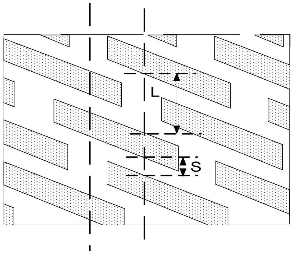
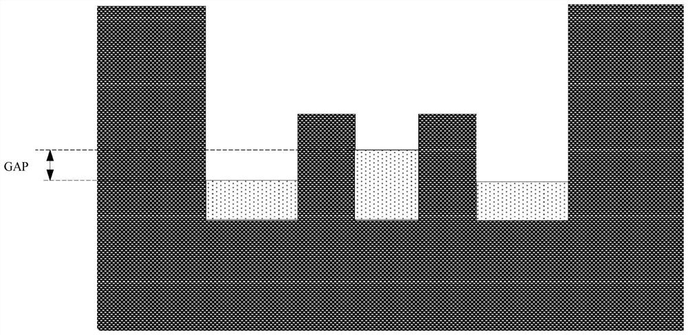
technical field [0001] The present invention relates to the technical field of semiconductor fabrication technology, in particular to a buried gate structure and a fabrication method thereof. Background technique [0002] As one of the necessary components in integrated circuits, gates play the role of switches in circuits and are widely used in integrated circuits. [0003] Please also see figure 1 and figure 2 , With the shrinking of the structure size of semiconductor devices, in order to further increase the density of active regions in the manufacture of integrated circuits below 20nm, the active regions are arranged in a parallel and staggered manner, so that in the process of etching the gate trenches Encounter shallow trench isolation (Shallow Trench Isolation, STI) structures with different widths, such as figure 1 The width of the shallow trench in the L (Long) region is larger than the trench width in the S (Short) region. like figure 2 shown, the grooves o...

Claims


Application Information

Patent Timeline
Patent Type & Authority Patents(China)
IPC IPC(8): H01L21/3065H01L21/28H01L29/423
CPCH01L21/3065H01L29/401H01L29/4236
Inventor 不公告发明人
Owner CHANGXIN MEMORY TECH INC
Learn More