Manufacturing method of light-emitting unit and manufacturing device of light-emitting unit

A technology for a light-emitting unit and a manufacturing method, which is applied in the direction of electrical components, semiconductor/solid-state device manufacturing, and circuits, and can solve problems such as increasing the shading area, reducing the light output ratio, and being unable to exit the light-emitting surface, so as to reduce the shading area and improve The effect of light ratio

Inactive Publication Date: 2021-04-23
BEIJING IVISUAL 3D TECH CO LTD
View PDF5 Cites 0 Cited by
  • Summary
  • Abstract
  • Description
  • Claims
  • Application Information

AI Technical Summary

Problems solved by technology

[0004] like figure 1 As shown, the length L1 of the ohmic contact layer 11 made by the current process is longer than the length L2 of the cross-section of the electrode 12 arranged on the ohmic contact layer 11, which increases the shading area, so that direct emission and reflection pass through the ohmic contact layer The light near 11 is blocked by the ohmic contact layer 11, and cannot be emitted to the light-emitting surface, which reduces the light-emitting ratio

Method used


Image

  • Manufacturing method of light-emitting unit and manufacturing device of light-emitting unit
  • Manufacturing method of light-emitting unit and manufacturing device of light-emitting unit
  • Manufacturing method of light-emitting unit and manufacturing device of light-emitting unit

Examples


Embodiment Construction

[0070] In order to understand the characteristics and technical content of the embodiments of the present disclosure in more detail, the implementation of the embodiments of the present disclosure will be described in detail below in conjunction with the accompanying drawings. The attached drawings are only for reference and description, and are not intended to limit the embodiments of the present disclosure. In the following technical description, for purposes of explanation, numerous details are set forth in order to provide a thorough understanding of the disclosed embodiments. However, at least one embodiment can be practiced without these details. In other instances, well-known structures and devices may be shown simplified in order to simplify the drawings.

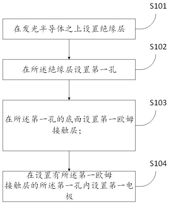
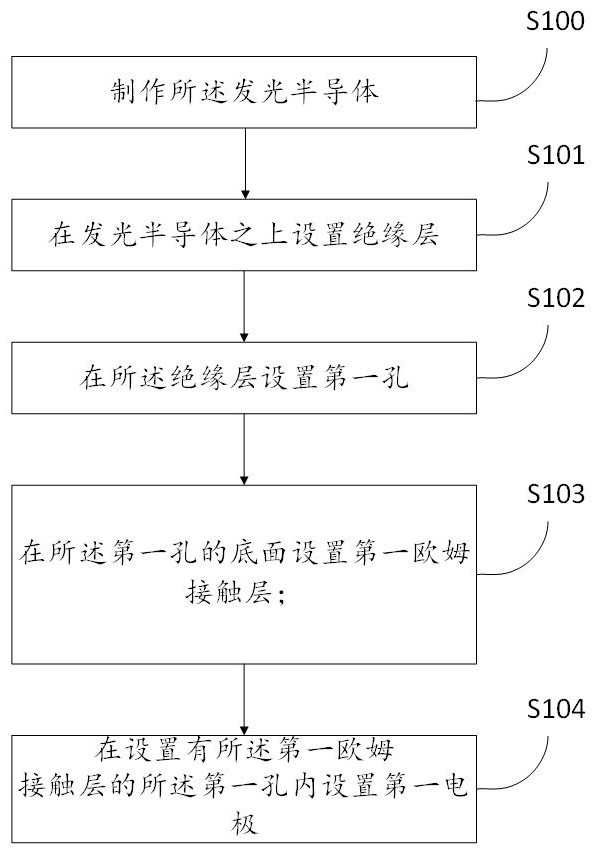
[0071] Such as figure 2 As shown, the embodiment of the present disclosure provides a manufacturing method of the light emitting unit 100, including:

[0072] S101: disposing an insulating layer 101 on the light-...


PUM


Abstract

The invention relates to the technical field of semiconductors, and discloses a manufacturing method of a light-emitting unit; the method comprises the following steps: arranging an insulating layer on a light-emitting semiconductor, the light-emitting semiconductor comprising a second semiconductor layer, an active layer and a first semiconductor layer which are sequentially laminated from one side close to the insulating layer to one side far away from the insulating layer; arranging a first hole in the insulating layer; arranging a first ohmic contact layer on the bottom surface of the first hole; and arranging a first electrode in the first hole provided with the first ohmic contact layer; one surface, far away from the light-emitting semiconductor, of the insulating layer is located above the plane where the first surface of the second semiconductor layer is located. According to the manufacturing method provided by the invention, the length of the first ohmic contact layer can be kept consistent with the length of the cross section of the first electrode, and the light emitting proportion is improved. The invention further discloses a manufacturing device of the light-emitting unit.

Description

technical field [0001] The present application relates to the technical field of semiconductors, for example, to a method for manufacturing a light emitting unit and a device for manufacturing a light emitting unit. Background technique [0002] At present, when making a light-emitting unit, it is usually necessary to arrange an ohmic contact layer between the semiconductor layer and the electrode to form an ohmic contact. [0003] In the process of implementing the embodiments of the present disclosure, it is found that at least the following problems exist in related technologies: [0004] Such as figure 1 As shown, the length L1 of the ohmic contact layer 11 made by the current technology is longer than the length L2 of the cross-section of the electrode 12 arranged on the ohmic contact layer 11, which increases the light-shielding area, so that direct emission and reflection pass through the ohmic contact layer The light near 11 is blocked by the ohmic contact layer 11...

Claims


Application Information

Patent Timeline
IPC IPC(8): H01L33/36H01L33/38H01L21/768
CPCH01L21/76877H01L21/76895H01L33/36H01L33/38
Inventor 不公告发明人
Owner BEIJING IVISUAL 3D TECH CO LTD
Why Eureka
Try Eureka