Micro LED chip, growth substrate, display panel and micro LED chip transfer method

A technology for LED chips and growth substrates, which is applied in the manufacture of semiconductor devices, electrical components, semiconductor/solid-state devices, etc., can solve the problems that micro-LED chips are not easy to be picked up, reduce the probability of crushing, high transfer efficiency, and easy transfer effect

Active Publication Date: 2021-04-30
CHENGDU VISTAR OPTEOLECTRONICS CO LTD
View PDF8 Cites 0 Cited by
  • Summary
  • Abstract
  • Description
  • Claims
  • Application Information

AI Technical Summary

Problems solved by technology

[0004] In the prior art, there is a problem that micro LED chips are not easy to be picked up during the transfer process

Method used


Image

  • Micro LED chip, growth substrate, display panel and micro LED chip transfer method
  • Micro LED chip, growth substrate, display panel and micro LED chip transfer method
  • Micro LED chip, growth substrate, display panel and micro LED chip transfer method

Examples


Embodiment Construction

[0026] The following will clearly and completely describe the technical solutions in the embodiments of the present application with reference to the drawings in the embodiments of the present application. Obviously, the described embodiments are only some of the embodiments of the present application, not all of them. Based on the embodiments in this application, all other embodiments obtained by persons of ordinary skill in the art without making creative efforts belong to the scope of protection of this application.

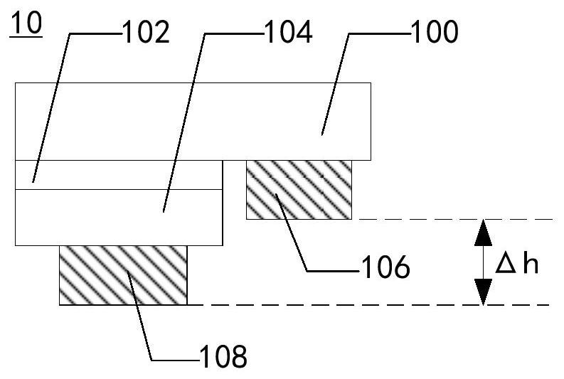
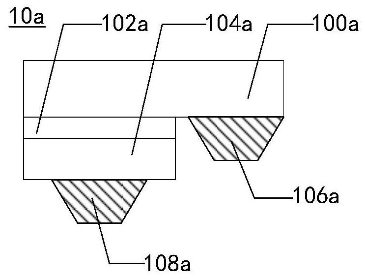
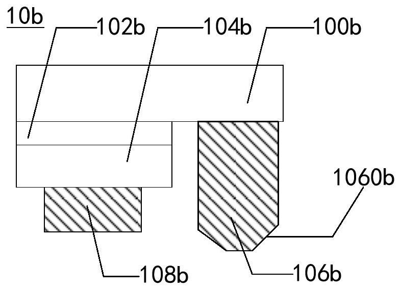
[0027] The inventors of the present application found in the long-term research process that the specific process of laser lift-off is: firstly, a plurality of micro-LED chips with a transparent substrate are completely pressed into the bonding layer, so that the plurality of micro-LED chips are bonded The composite layer is fixed; then the laser is irradiated from one side of the transparent substrate, so that a plurality of micro LED chips are separated from ...


PUM


Abstract

The invention discloses a micro LED chip, a growth substrate, a display panel and a micro LED chip transfer method. The micro LED chip comprises: a first doped epitaxial layer which comprises a first region and a second region; a light-emitting layer which at least covers part of the first area; a second doped epitaxial layer which covers the surface of one side, far away from the first doped epitaxial layer, of the light emitting layer; a first electrode arranged in the second region and positioned on the same side as the light-emitting layer; and a second electrode arranged on the side, away from the light-emitting layer, of the second doped epitaxial layer, wherein the orthographic projections of the first electrode and the second electrode on the first doped epitaxial layer do not coincide. The first electrode and the second electrode have a height difference in the thickness direction of the micro LED chip, and the height difference is larger than 0.5 micrometer and smaller than 3 micrometers. By means of the mode, the micro LED chip can be not completely sunken into the bonding layer after laser stripping, and transferring is easy.

Description

technical field [0001] The present application relates to the field of display technology, in particular to a method for transferring a micro LED chip, a growth substrate, a display panel and a micro LED chip. Background technique [0002] Micro LED (Light Emitting Diode, Light Emitting Diode) chip display technology has the advantages of high brightness, high response speed, low power consumption, long life, etc., and has become a research hotspot for people to pursue a new generation of display technology. [0003] At present, in the preparation process of micro-LED display panels, laser lift-off and batch transfer are two very important processes. The specific process of batch transfer is: using the transfer head to transfer multiple micro LED chips. [0004] In the prior art, there is a problem that micro LED chips are not easy to be picked up during the transfer process. Contents of the invention [0005] The technical problem mainly solved by this application is to...

Claims


Application Information

Patent Timeline
Patent Type & Authority Applications(China)
IPC IPC(8): H01L33/38H01L27/15H01L21/67H01L33/00H01L33/48
CPCH01L33/38H01L27/156H01L21/67144H01L33/48H01L2933/0033
Inventor 姚志博夏继业董小彪王程功
Owner CHENGDU VISTAR OPTEOLECTRONICS CO LTD
Why Eureka
Try Eureka