Internally-packaged digital chip LED and packaging method thereof

A digital chip and packaging method technology, which is applied in the direction of printed circuits, printed circuits, and electric solid devices connected to non-printed electrical components, can solve the problem that the surface position of the PCB board is relatively large, and save connection work, The effect of reducing the difficulty of wiring and reducing the occupied space

Pending Publication Date: 2021-05-25
SHENZHEN TIANCHENG LIGHTING CO LTD
View PDF4 Cites 0 Cited by
  • Summary
  • Abstract
  • Description
  • Claims
  • Application Information

AI Technical Summary

Problems solved by technology

[0004] In view of the above-mentioned related technologies, the inventor believes that: during the use of the lamp board, the use of the lamp beads needs to use the corresponding control chip to control the display state; install the lamp beads and the chip on the PCB board, and connect the chip and the lamp bead They are connected to the PCB board one by one; however, the above method of lamp bead and chip installation will lead to a large proportion of the surface of the PCB board. When multiple lamp beads are installed on the PCB board, the required surface area of ​​the PCB board will also increase, and the production The materials required for the light board increase synchronously, and this situation needs to be further improved

Method used


Image

  • Internally-packaged digital chip LED and packaging method thereof
  • Internally-packaged digital chip LED and packaging method thereof
  • Internally-packaged digital chip LED and packaging method thereof

Examples


Embodiment Construction

[0041] The following is attached Figure 1-4 , to further describe this application in detail.

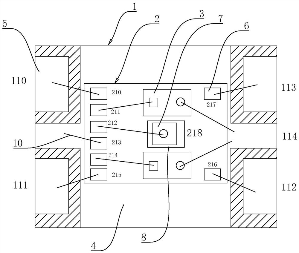
[0042] When welding the LED lamp bead to the corresponding PCB board, the light-emitting chip 3 and the control chip inside the lamp bead need to be welded on the PCB board, in order to reduce the occupied space of the light-emitting chip 3 and the control chip on the plane of the PCB board.

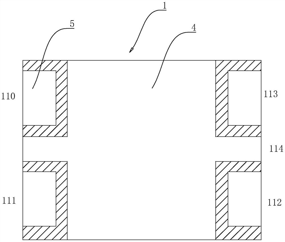
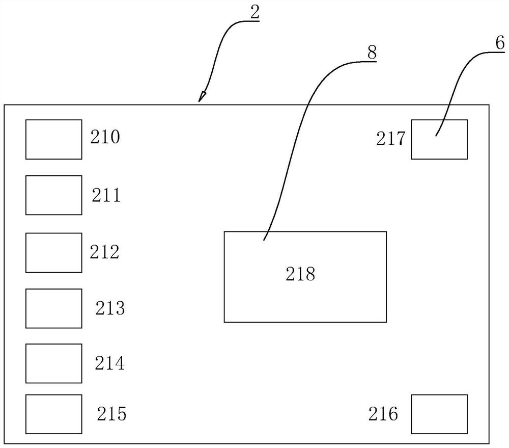
[0043] The embodiment of the present application discloses an internally sealed digital chip LED, refer to figure 1 and figure 2 , including package carrier 1, digital chip 2 and light-emitting chip 3 connected to the PCB board, when the lamp beads are welded on the PCB board, the package bottom plate is welded on the PCB board, and the digital chip 2 is set on the package carrier 1 On the side away from the PCB board, in order to realize the electrical connection between the package bottom plate and the digital chip 2, the package carrier 1 is provided with a second metal pad 4 in the mid...


PUM


Abstract

The invention relates to the field of lighting display devices, in particular to an internally-packaged digital chip LED which comprises a packaging carrier connected to a PCB, a digital chip and a light-emitting chip, the digital chip is arranged on the side, away from the PCB, of the packaging carrier, the packaging carrier is electrically connected with the digital chip, the light-emitting chip is arranged on the side, away from the packaging carrier, of the digital chip, the light-emitting chip is electrically connected with the digital chip, and the packaging carrier, the digital chip and the light-emitting chip are sequentially arranged in a stacked mode from bottom to top. According to the invention, the installation space of the lamp beads on the PCB and the plane position of the corresponding digital chip is saved, so that the size of the required PCB can be reduced.

Description

technical field [0001] The present application relates to the field of lighting display devices, in particular to an inner-enclosed digital chip LED and a packaging method thereof. Background technique [0002] With the advancement of social science and technology, the current lighting display equipment is becoming more and more abundant, and all kinds of lighting devices are free to buy and use. Among them, the most widely used one is LED light display. LED light is light-emitting diode, which uses solid semiconductor chips. It is a luminescent material. Compared with traditional lamps, LED lamps are energy-saving, environmentally friendly, and have better color rendering and response speed. [0003] LED lights are also suitable for overall display. They can be installed on a light board according to a pre-designed arrangement. By assembling the LED light-emitting chip with the light board according to the pre-designed circuit wiring PCB board, and then through the external...

Claims


Application Information

Patent Timeline
IPC IPC(8): H01L25/16H01L33/48H01L33/62H05K1/18
CPCH01L25/167H01L33/483H01L33/62H05K1/185H05K2201/10106
Inventor 林坚耿李浩锐金国奇
Owner SHENZHEN TIANCHENG LIGHTING CO LTD
Why Eureka
Try Eureka