PCB dielectric slice selection method, device and system

A technology of PCB board and dielectric sheet, applied in the field of PCB board dielectric sheet selection method, device and system, which can solve the problems of increasing design cost, reducing the utilization rate of board materials, layer deviation or sliding board of multiple media, and achieving suppression of common mode Voltage, low cost, and the effect of improving signal eye diagram quality

Pending Publication Date: 2021-06-04
LANGCHAO ELECTRONIC INFORMATION IND CO LTD
View PDF3 Cites 0 Cited by
  • Summary
  • Abstract
  • Description
  • Claims
  • Application Information

AI Technical Summary

Problems solved by technology

[0005] 1) Choose the type of glass fiber cloth with relatively dense glass fiber cloth window, but the disadvantage is that it will increase the design cost;
[0006] 2) Rotate the differential line at a certain angle for wiring (usually 10° winding), or rotate the plate directly during processing after the normal warp and weft wiring is completed. Although the glass fiber effect can be reduced, the utilization rate of the plate is reduced. ;
[0007] 3) Choose to use multiple media sheets of the same specification to be stacked together. From the perspective of probability, the probability of empty windows is very small when the same windowed media sheets are stacked together, but the disadvantage is that multiple media sheets There may be a risk of layer deviation or slippage during PCB lamination

Method used


Image

  • PCB dielectric slice selection method, device and system
  • PCB dielectric slice selection method, device and system
  • PCB dielectric slice selection method, device and system

Examples


Embodiment Construction

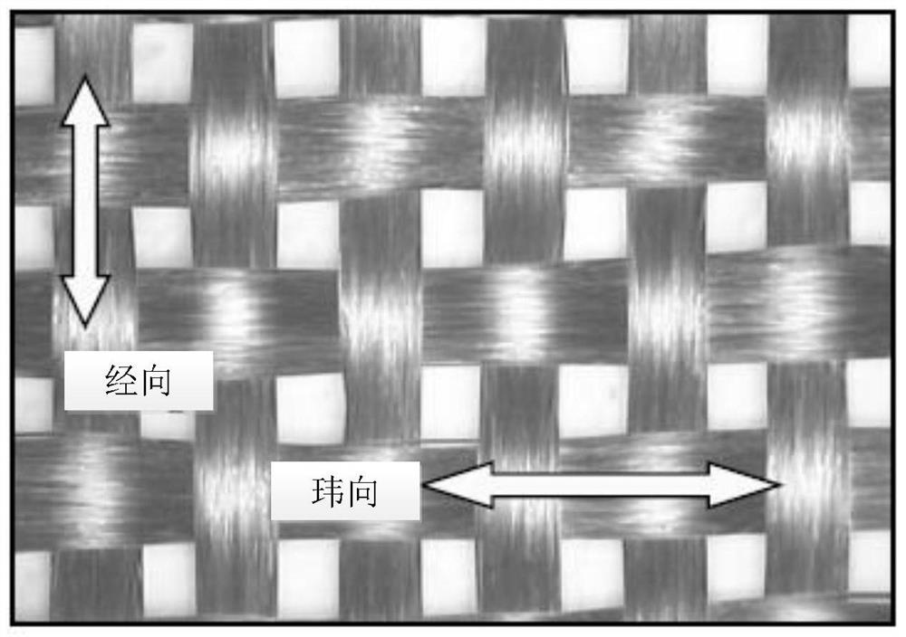
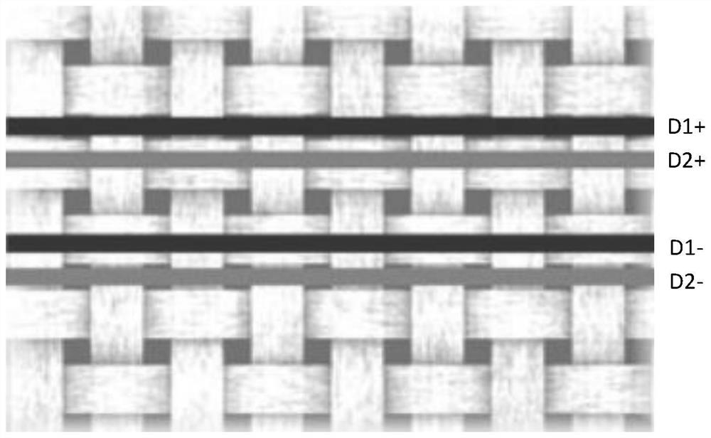
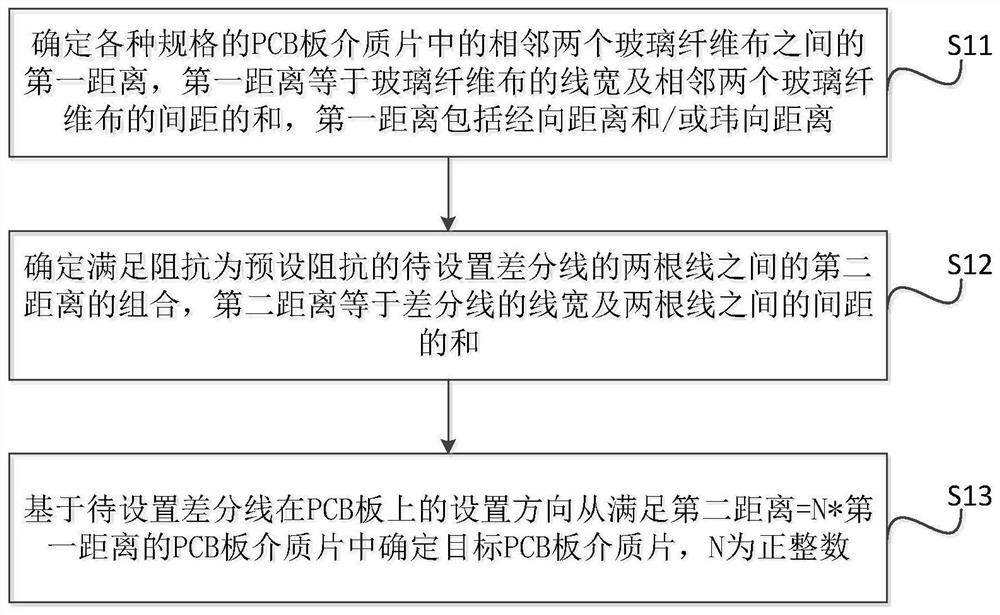
[0050] The core of the present invention is to provide a method, device and system for selecting a PCB dielectric sheet, which avoids the differential skew effect brought by the glass fiber effect, suppresses the common-mode voltage, thereby reducing system crosstalk and EMI interference, and improving the quality of the signal eye diagram , In addition, the cost is low, which ensures the utilization rate of the plate and high reliability.

[0051] In order to make the purpose, technical solutions and advantages of the embodiments of the present invention clearer, the technical solutions in the embodiments of the present invention will be clearly and completely described below in conjunction with the drawings in the embodiments of the present invention. Obviously, the described embodiments It is a part of embodiments of the present invention, but not all embodiments. Based on the embodiments of the present invention, all other embodiments obtained by persons of ordinary skill ...


PUM


Abstract

The invention discloses a PCB dielectric slice selection method, device and system, and the method comprises the steps: determining a first distance between two pieces of adjacent glass fiber cloth in PCB dielectric slices of various specifications, and then determining a combination of a second distance between two lines of a to-be-set differential line, the impedance of which is preset impedance; subsequently determining the target PCB dielectric sheet from the PCB dielectric sheets satisfying the second distance = N * first distance according to the setting direction of the differential line to be set on the PCB, so that the second distance = N * first distance, the impedance of the PCB dielectric sheets through which the two lines of the differential line pass is the same. Therefore, the two lines generate the same signal delay, the difference Skew influence caused by the glass fiber effect is avoided, the common-mode voltage is inhibited, the system crosstalk and EMI interference are reduced, the signal eye pattern quality is improved, in addition, the cost is low, the utilization rate of the plate is ensured, and the reliability is high.

Description

technical field [0001] The invention relates to the technical field of PCB boards, in particular to a method, device and system for selecting a PCB dielectric sheet. Background technique [0002] For digital signals transmitted on PCB (Printed Circuit Board, Chinese name is printed circuit board) board, many dielectric materials, including FR4, used in the electronics industry have always been considered uniform in low-speed and low-frequency signal transmission. . But when the digital signal rate on the transmission line reaches the Gbps level, this assumption of uniformity is no longer valid. The reasons are as follows: [0003] The PCB board dielectric sheet includes glass fiber cloth and resin. Among them, the glass fiber cloth is like a skeleton, which plays the role of increasing strength and support. The resin has fluidity like glue, which plays a bonding effect. Therefore, if you encounter such figure 1 After the window is opened in the middle of the glass fiber c...

Claims


Application Information

Patent Timeline
IPC IPC(8): H05K3/00H05K13/00
CPCH05K3/0011H05K13/00
Inventor 李健
Owner LANGCHAO ELECTRONIC INFORMATION IND CO LTD
Why Eureka
Try Eureka