
LED silica gel module manufacturing process

A manufacturing process and silicone mold technology, applied in the field of LED silicone module manufacturing process, can solve the problems of complex manufacturing process operation, glue weighing and preheating, glue waste molding and other problems, to improve product quality, easy operation, avoid glue wasteful effect

Pending Publication Date: 2021-06-15
钱丽君
View PDF0 Cites 0 Cited by
  • Summary
  • Abstract
  • Description
  • Claims
  • Application Information

AI Technical Summary

Problems solved by technology

[0004] The purpose of the present invention is to solve the complicated operation of the existing LED silica gel production process. The glue is not weighed and preheated before the glue injection, which is easy to cause glue waste and slow molding. At the same time, there is no surface treatment for the LED silica gel after molding. , the shortcomings that affect product quality, and the proposed LED silicone module manufacturing process

Method used


Image

  • LED silica gel module manufacturing process
  • LED silica gel module manufacturing process

Examples


Embodiment 1

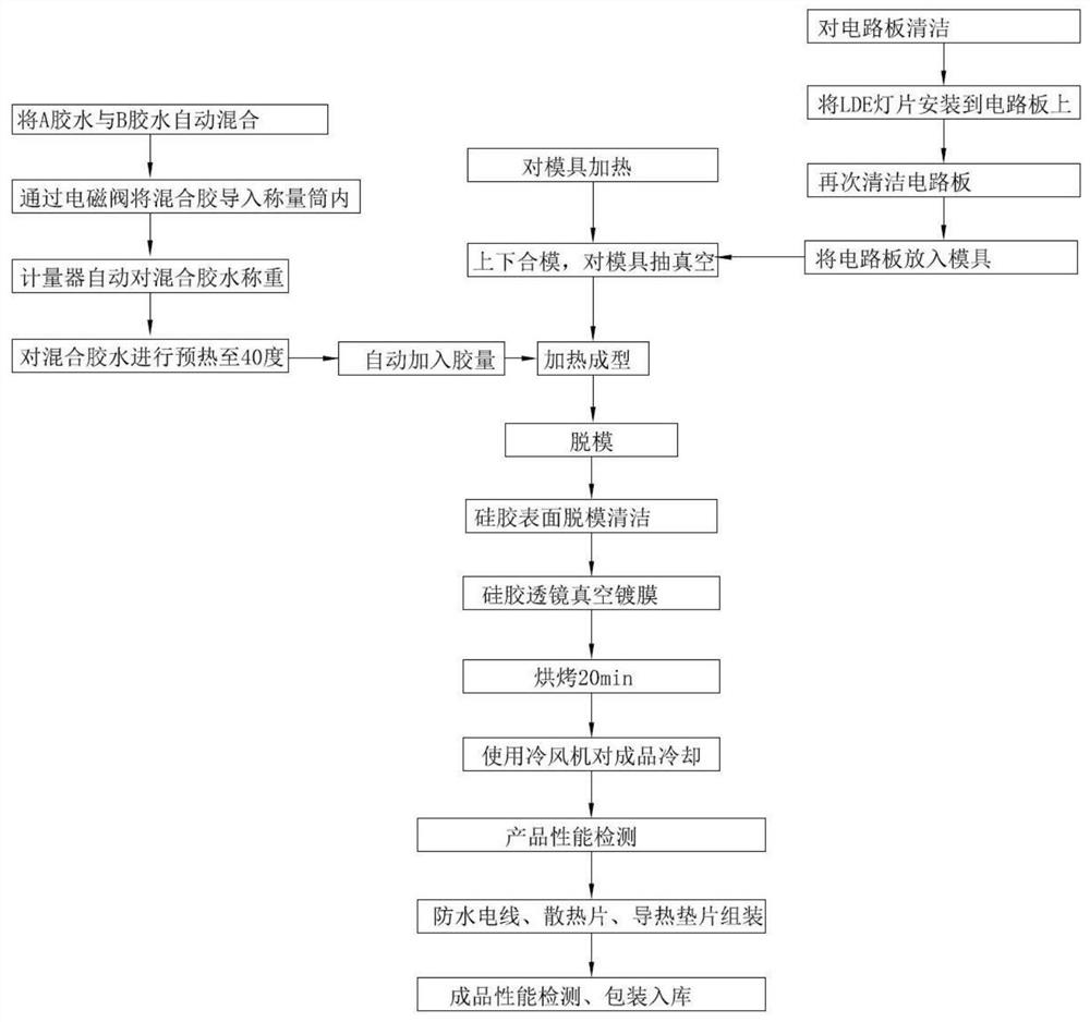
[0037] refer to Figure 1-2 , LED silicone module manufacturing process, including the following process steps:

[0038] S1: Mix glue A and glue B, and defoam;

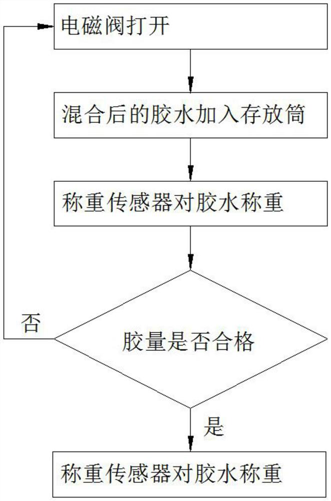
[0039] S2: Import the mixed glue into the storage cylinder for storage;

[0040] S3: Quantitatively import the mixed glue in the storage cylinder into the weighing cylinder for weighing;

[0041] S4: Preheating the weighed mixed glue;

[0042] S5: pretreating the mould;

[0043] S6: Pretreat the circuit board and put it into the mold;

[0044] S7: Automatically add the weighed and preheated mixed glue, and heat to shape;

[0045] S8: demoulding;

[0046] S9: Silica gel molding surface treatment;

[0047] S10: cooling and product testing;

[0048] S11: assembly;

[0049] S12: Product testing, packaging and storage.

[0050] In this example, the ratio of A glue to B glue in S1 is 1:1, put A glue and B glue into two barrels, and the automatic stirring time is one minute. The time is one minute, and the air bub...

Embodiment 2

[0060] refer to Figure 1-2 , LED silicone module manufacturing process, including the following process steps:

[0061] S1: Mix glue A and glue B, and defoam;

[0062] S2: Import the mixed glue into the storage cylinder for storage;

[0063] S3: Quantitatively import the mixed glue in the storage cylinder into the weighing cylinder for weighing;

[0064] S4: Preheating the weighed mixed glue;

[0065] S5: pretreating the mould;

[0066] S6: Pretreat the circuit board and put it into the mold;

[0067] S7: Automatically add the weighed and preheated mixed glue, and heat to shape;

[0068] S8: demoulding;

[0069] S9: Silica gel molding surface treatment;

[0070] S10: cooling and product testing;

[0071] S11: assembly;

[0072] S12: Product testing, packaging and storage.

[0073] In this example, the ratio of A glue to B glue in S1 is 1:1, put A glue and B glue into two barrels, and the automatic stirring time is one minute. The time is one minute, and the air bubbl...


PUM


Abstract

The invention belongs to the technical field of silica gel module manufacturing, particularly relates to an LED silica gel module manufacturing process, and aims to solve the problems that an existing LED silica gel manufacturing process is complex in operation, glue is not weighed and preheated before glue injection, glue waste is easily caused, forming is slow, meanwhile, surface treatment is not carried out on formed LED silica gel, and product quality is affected. Now the following scheme is put forwards, the method comprises the following process steps that S1, glue A and glue B are mixed, and defoaming is conducted; S2, the mixed glue is guided into a storage barrel to be stored; S3, quantitatively guiding the mixed glue in the storage barrel into a weighing barrel for weighing; S4, the weighed mixed glue is pre-heated; and S5, a mold is pretreated. The method is convenient to operate, the glue is weighed and preheated before glue injection, glue waste and slow forming are avoided, the formed LED silica gel is subjected to surface treatment, and the product quality is improved.

Description

technical field [0001] The invention relates to the technical field of silica gel module manufacturing, in particular to a manufacturing process of LED silica gel modules. Background technique [0002] LED silicone is the general term for organic silicone materials in the LED photoelectric industry. Due to the weak anti-ozone ability of epoxy, the colloid turns yellow, which affects the light transmission effect, while the silica gel material has excellent properties such as anti-atmospheric aging and ultraviolet aging, and its processing method is mainly made by heating and forming a mold. [0003] The existing LED silica gel manufacturing process is complicated to operate. The glue is not weighed and preheated before the glue is injected, which is likely to cause glue waste and slow molding. At the same time, there is no surface treatment of the LED silica gel after molding, which affects product quality. Contents of the invention [0004] The purpose of the present inv...

Claims


Application Information

Patent Timeline
Patent Type & Authority Applications(China)
IPC IPC(8): B29C45/14B29C45/00B29C45/17
CPCB29C45/0055B29C45/14008B29C45/1701
Inventor 钱丽君
Owner 钱丽君
Learn More