
Deep learning chip packaging crack defect detection method based on YOLO

A defect detection and chip packaging technology, which is applied in neural learning methods, image data processing, image enhancement, etc., can solve the problems of slow detection speed of YOLO network, difficulty in meeting industrial detection, and affecting detection effect, so as to improve network prediction speed, Good detection effect, reduce the effect of false prediction frequency

Active Publication Date: 2021-06-15
SHENZHEN GRADUATE SCHOOL TSINGHUA UNIV
View PDF9 Cites 14 Cited by
  • Summary
  • Abstract
  • Description
  • Claims
  • Application Information

AI Technical Summary

Problems solved by technology

[0008] The defect detection method based on deep learning has the advantages of simple intelligence, high flexibility, good universality, and low hardware requirements. However, in the training phase of the network model, a sufficient number of defect samples need to be provided to the network for learning, and the chip The number of defect samples in the production process is very small, and the number of defect samples is too small to easily lead to over-fitting of the network model and affect the detection effect
The YOLO network is proposed for general target detection. When the YOLO network is directly used for chip defect detection, it will ignore the chip defect distribution with template information. There is still room for improvement in the accuracy of defect detection, and the existing YOLO network detection speed is relatively low. Slow, difficult to meet the needs of industrial testing

Method used


Image

  • Deep learning chip packaging crack defect detection method based on YOLO
  • Deep learning chip packaging crack defect detection method based on YOLO
  • Deep learning chip packaging crack defect detection method based on YOLO

Examples


Embodiment Construction

[0037] Embodiments of the present invention will be described in detail below. It should be emphasized that the following description is exemplary only, and is not intended to limit the scope of the invention and its application.

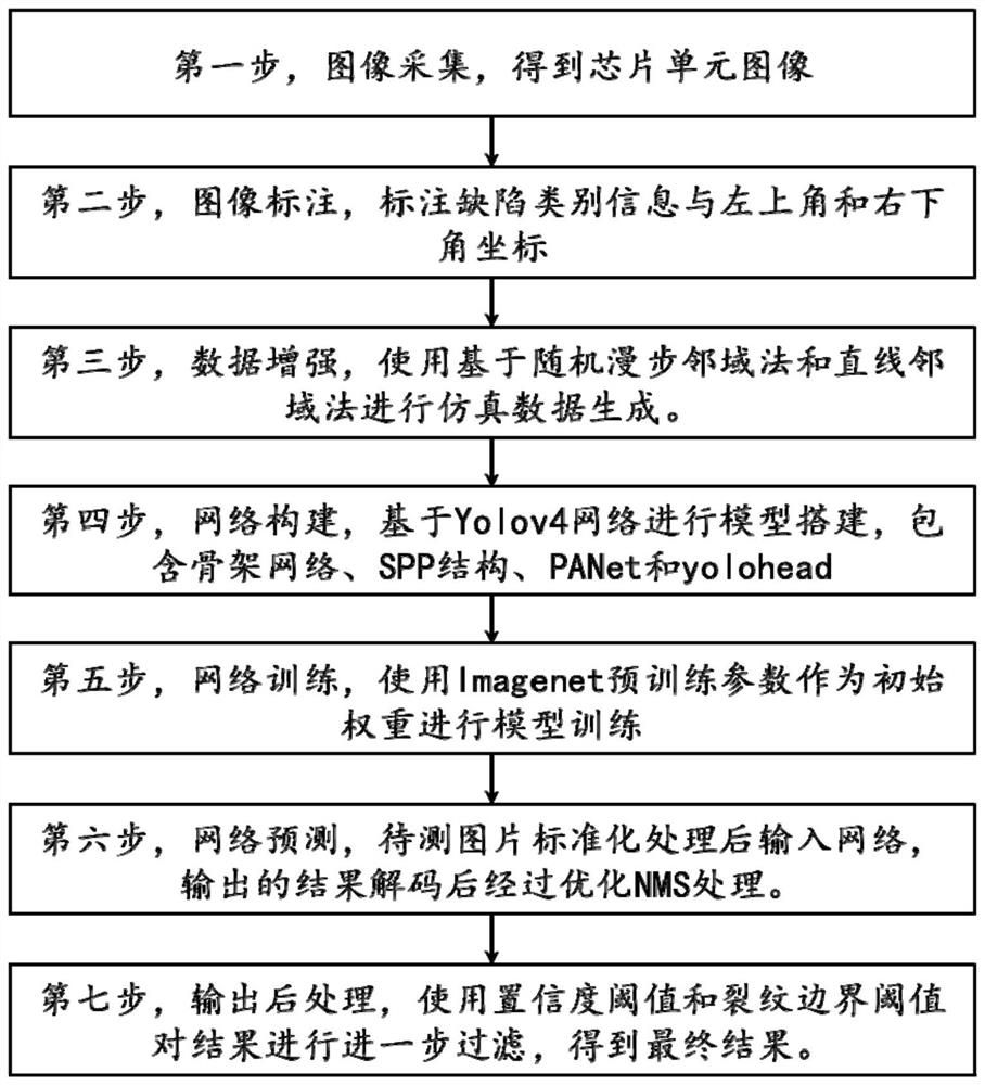
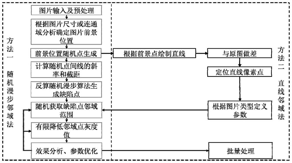
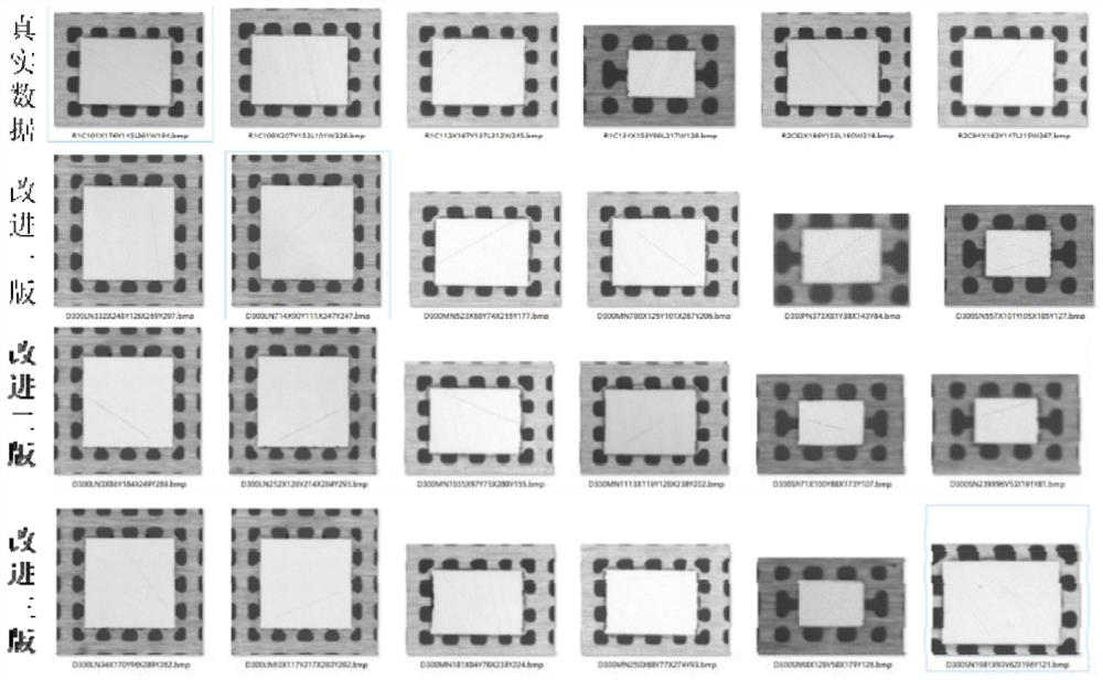
[0038] In order to correctly distinguish between good product pictures and crack pictures, the embodiment of the present invention provides a YOLO-based deep learning chip package crack defect detection method. The overall process of the method is as follows figure 1 As shown, it can be divided into seven steps: image acquisition, image annotation, data enhancement, model building, network training, network prediction and output post-processing.

[0039] The first step, image acquisition, collects industrial image data, and captures the image of the chip unit.

[0040] The second step, image labeling, uses an image labeling tool for labeling, and the labeling content is the defect category (ie crack) and the coordinates of the upper left and lower ...


PUM


Abstract

The invention discloses a deep learning chip packaging crack defect detection method based on YOLO. The method comprises the following steps: 1, acquiring a chip unit image; step 2, labeling defect category information and defect target coordinates for the acquired image; 3, performing data enhancement, and making a data set for training; 4, constructing a deep learning network model used for defect detection based on a YOLOv4 network; 5, training the deep learning network by using the pre-trained parameters as initial weights; 6, using the trained network for prediction, standardizing a to-be-detected picture, inputting the standardized to-be-detected picture into the network to obtain the output of a network head, decoding the head output, and using an optimized non-maximum suppression (NMS) to filter a decoded result to obtain a network prediction result; and 7, further filtering the network prediction result in the step 6 by adopting a confidence coefficient threshold value and a crack boundary threshold value to obtain a final result. The method has a good detection effect on chip crack defects.

Description

technical field [0001] The invention relates to chip package defect detection, in particular to a YOLO-based deep learning chip package crack defect detection method. Background technique [0002] Chips are the core components of the electronics industry, and a large number of unusable defective products will be produced due to defects in the large-scale production of chips. Among them, the main defects will appear on the surface of the chip, and different types of defects are accompanied by different appearance features such as cracks. An important part of the packaging test is to detect defects on the surface of the chip. Chip packaging and testing is an important link to eliminate defective products and ensure product quality and production reliability. Emerging fields such as artificial intelligence, Internet of Things, and cloud computing are inseparable from high-end advanced packaging and testing technologies. Because chip surface defects have appearance characterist...

Claims


Application Information

Patent Timeline
IPC IPC(8): G06T7/00G06T7/13G06T7/136G06T7/62G06T7/73G06K9/62G06N3/04G06N3/08
CPCG06T7/0004G06T7/13G06T7/136G06T7/62G06T7/73G06N3/08G06T2207/10004G06T2207/30148G06N3/045G06F18/24
Inventor 曾龙王宏羽杨凡王硕林宜龙刘飞
Owner SHENZHEN GRADUATE SCHOOL TSINGHUA UNIV
Learn More