
Display device

A display device and display panel technology, applied in static indicators, nonlinear optics, instruments, etc., can solve problems such as surface material variation, ink layer performance impact, panel performance impact, etc., to achieve high-precision values, ensure quality and performance Effect

Inactive Publication Date: 2021-06-18
WUHAN CHINA STAR OPTOELECTRONICS TECH CO LTD
View PDF6 Cites 0 Cited by
  • Summary
  • Abstract
  • Description
  • Claims
  • Application Information

AI Technical Summary

Problems solved by technology

Specifically, in the terminal area, the surface test will be carried out on the exposed area of ​​the display device. The test method is to draw a line with a dyne stroke. If the dyne line shrinks, it proves that the surface material in this area has changed, which will affect the overall effect.
However, since the display panel is equipped with a buffer component, after the buffer component contacts the ink layer, the material in the buffer component will chemically react with the ink layer, which will affect the performance of the ink layer, resulting in the inability to accurately estimate the quality of the display panel. conduct assessment
And when the ink layer is bonded with other film layers, it is prone to problems such as loose bonding or even tearing, which will affect the performance of the panel
[0004] To sum up, when testing the performance of the display device, the cushioning components installed inside the display device are likely to react with the ink layer, thereby affecting the performance of the ink layer and the dyne value of the panel. At the same time, the affected ink layer is in the When bonding with other film layers, it is prone to problems such as loose bonding or even tearing

Method used


Image

  • Display device
  • Display device
  • Display device

Examples


Embodiment Construction

[0028] The following will clearly and completely describe the technical solutions in the embodiments of the present invention with reference to the drawings in the embodiments of the present invention. Apparently, the described embodiments are only some of the embodiments of the present invention, but not all of them. Based on the embodiments of the present invention, all other embodiments obtained by those skilled in the art without creative efforts fall within the protection scope of the present invention.

[0029] In describing the present invention, it should be understood that the terms "center", "longitudinal", "transverse", "length", "width", "thickness", "upper", "lower", "front", " Orientation indicated by rear, left, right, vertical, horizontal, top, bottom, inside, outside, clockwise, counterclockwise, etc. The positional relationship is based on the orientation or positional relationship shown in the drawings, which is only for the convenience of describing the pr...


PUM


Abstract

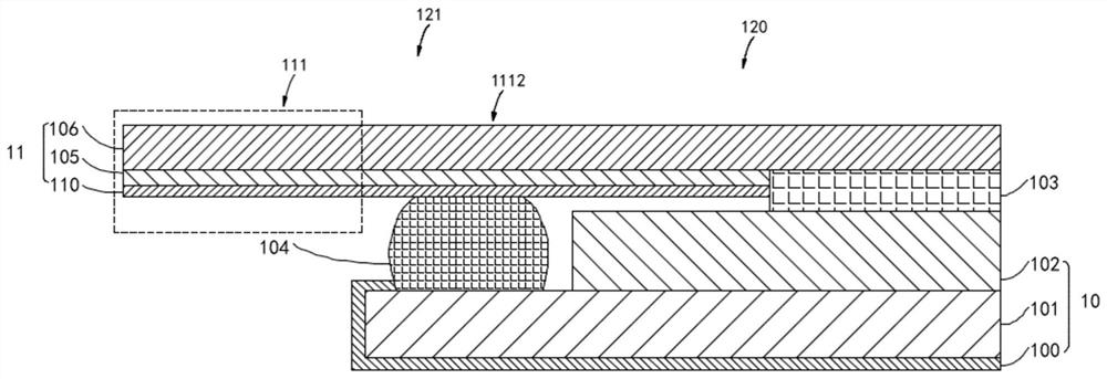
The invention provides a display device which comprises a cover plate and a display panel, the display panel and the cover plate are oppositely arranged, the cover plate further comprises an ink layer and a protective layer, the ink layer is arranged on the cover plate, the protective layer is arranged on the side face, away from the cover plate layer, of the ink layer, and meanwhile a buffer component is arranged in the display device. One end of the buffer component is connected with the display panel, and the other end of the buffer component is connected with the protective layer. According to the display panel, the ink layer and the protective layer are arranged on one side of the cover plate layer, so that the influence of materials in the buffer component on the ink layer is effectively prevented, the problems that the ink layer is not tightly connected with other film layers and is easy to tear and the like are solved, and meanwhile, the accuracy of the display panel during dyne value testing and the quality of the display panel are ensured.

Description

[0001] The invention relates to the field of display panel manufacturing, in particular to a display device. Background technique [0002] With the continuous improvement of display panel manufacturing technology, people also put forward higher requirements on the quality and performance of the display panel. [0003] In order to obtain a display device with higher performance, multiple tests need to be performed on various properties of the display panel during the preparation process of the panel, so as to ensure that the display device has higher reliability and higher display performance. During the manufacturing process of the display panel, a layer of ink or the like is often provided at the bottom edge area of ​​the panel to prevent external light from entering the panel. At the same time, a buffer layer is provided between the cover plate and the panel to prevent the display device from collapsing when dropped or under pressure. In the process of testing the display p...

Claims


Application Information

Patent Timeline
Patent Type & Authority Applications(China)
IPC IPC(8): G02F1/1333G02F1/13G02F1/133
CPCG02F1/133308G02F1/1333G02F1/1309G02F1/133
Inventor 张占东
Owner WUHAN CHINA STAR OPTOELECTRONICS TECH CO LTD
Learn More