Welding method of semiconductor device and semiconductor device

A welding method and semiconductor technology, applied in the fields of semiconductor devices, semiconductor/solid-state device components, and semiconductor/solid-state device manufacturing, etc., can solve the problems such as the inability to discharge air bubbles smoothly, the high welding void rate, and the reduction of welding quality.

Active Publication Date: 2021-06-18
度亘核芯光电技术(苏州)有限公司
View PDF19 Cites 1 Cited by
  • Summary
  • Abstract
  • Description
  • Claims
  • Application Information

AI Technical Summary

Problems solved by technology

[0004] The purpose of the present invention is to provide a welding method for semiconductor devices and semiconductor devices, so as to alleviate the technical problems that the air bubbles cannot be smoothly discharged during the welding process of the existing semiconductor devices, the welding void rate is high, and the welding quality is reduced.

Method used


Image

  • Welding method of semiconductor device and semiconductor device
  • Welding method of semiconductor device and semiconductor device
  • Welding method of semiconductor device and semiconductor device

Examples


Embodiment Construction

[0035] The technical solutions of the present invention will be described below in conjunction with examples, as will be described, as described in Examples of the present invention, not all of the embodiments of the invention. Based on the embodiments of the present invention, there are all other embodiments obtained without making creative labor without making creative labor premises.

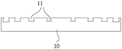
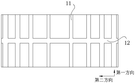
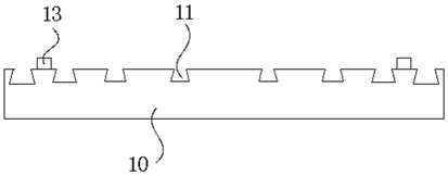
[0036] Such as Figures 1 to 7 As shown, the welding method of the semiconductor device provided in this embodiment, specifically includes the steps of:

[0037] Set the groove structure: a plurality of first grooves 11 extending in the first direction and disposed at the second direction in the surface of the first device 10, wherein in the second direction, in the middle of the first device 10 The width of the plurality of first recessed grooves 11 arranged in both sides gradually increases and between the adjacent two first recess 11 gradually decreases.

[0038]Deposition solder: A plurality o...


PUM

PropertyMeasurementUnit
widthaaaaaaaaaa

Abstract

The invention provides a welding method of a semiconductor device and a semiconductor device, and belongs to the technical field of semiconductor device preparation. The welding method comprises the following steps that a groove structure is set: a plurality of first grooves which extend along a first direction and are arranged at intervals along a second direction are formed on the surface of a first device; a solder is deposited; a solder structure is deposited on the surface of the first device, a plurality of protruding parts which extend in the first direction and are arranged at intervals in the second direction are formed on the surface of the solder structure, and the heights of the protruding parts are gradually reduced from the middle of the first device to the two sides of the first device in the second direction; the first device and a second device are welded; and the second device is placed on the solder structure, and the solder is heated, so that the second device can be soldered with the first device. In the welding process, the gaps between the adjacent protruding parts and the gap between the top faces of the protruding parts with the lower height and the second device can serve as exhaust channels, so that gas in the welding process is exhausted to the outside, cavities generated in a welded welding flux layer are reduced, and the void rate is reduced.

Description

Technical field [0001] The present invention relates to the field of preparation of semiconductor devices, and more particularly to a welding method of a semiconductor device and a semiconductor device. Background technique [0002] In the technical field of the semiconductor device, it is often encountered in the case of welding two devices. The quality of welding technology directly affects product quality and packaging efficiency. In some soldering, in order to improve production efficiency, it will be in one of them. The surface is first set, and then another device is placed above the solder and welded by heating. [0003] In the prior art, the gas generated by the solder and the air between the solder and the air between the devices are easily formed in the solder layer, and the contact area between the devices is large, so that the generated air bubble cannot be discharged smoothly, welded cavity High rate, reduce welding quality. Inventive content [0004] It is an objec...

Claims


Application Information

Patent Timeline
Patent Type & Authority Applications(China)
IPC IPC(8): H01L21/48H01L23/488
CPCH01L21/4814H01L21/4821H01L23/488H01L2224/83385
Inventor 惠利省李靖赵卫东
Owner 度亘核芯光电技术(苏州)有限公司
Why Eureka
Try Eureka