PCB (Printed Circuit Board) picking and placing device and PCB position correcting method

A PCB board and pick-and-place device technology, which is applied in the field of circuit board production equipment, can solve problems such as easy scratches on PCB boards, and achieve the effects of improving transfer efficiency, avoiding damage, and good use effects

Pending Publication Date: 2021-06-25
深圳市创新特科技有限公司
View PDF0 Cites 3 Cited by
  • Summary
  • Abstract
  • Description
  • Claims
  • Application Information

AI Technical Summary

Problems solved by technology

[0003] The purpose of the present invention is to provide a PCB pick-and-place device and a method for correcting the position of the PCB, aiming at solving the technical problem that the PCB is easily scratched during the process of correcting the position of the PCB in the prior art

Method used


Image

  • PCB (Printed Circuit Board) picking and placing device and PCB position correcting method
  • PCB (Printed Circuit Board) picking and placing device and PCB position correcting method
  • PCB (Printed Circuit Board) picking and placing device and PCB position correcting method

Examples


Embodiment Construction

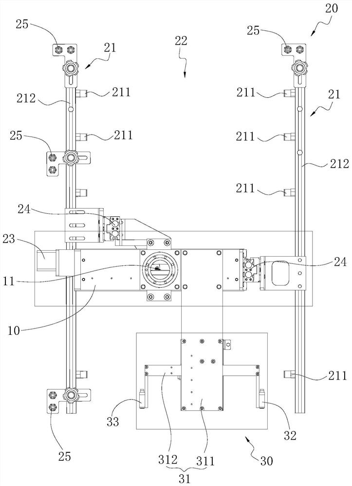
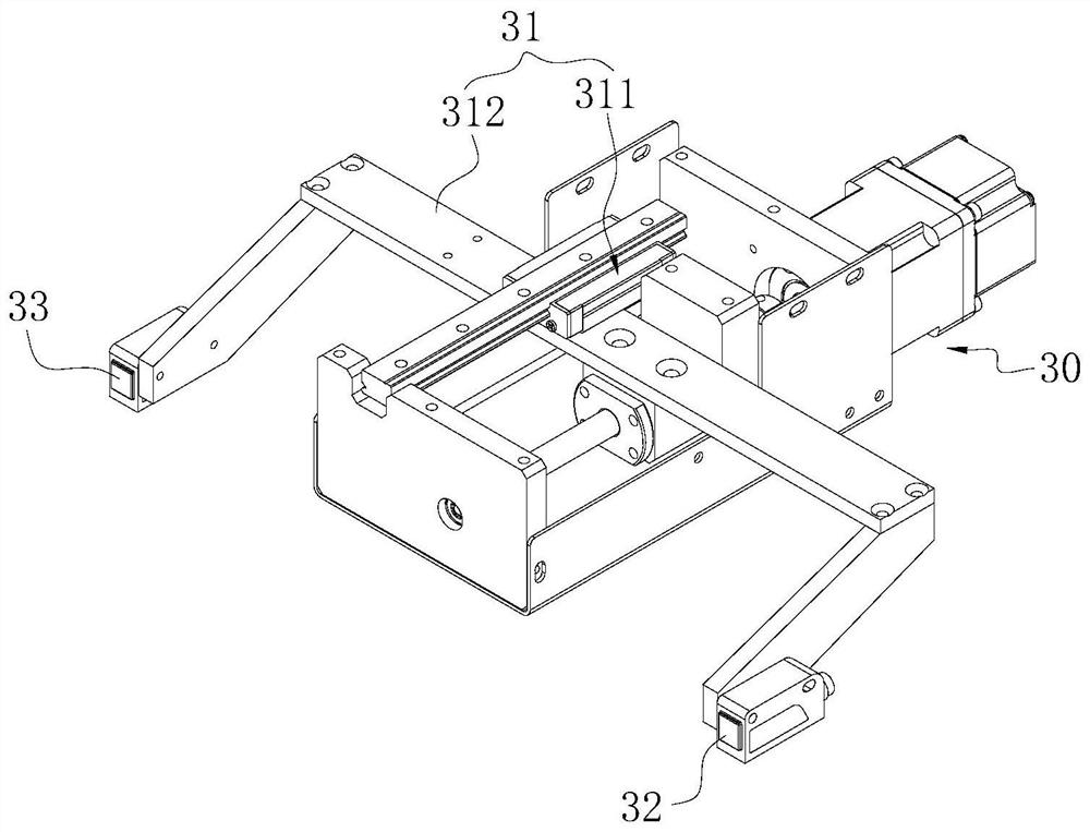
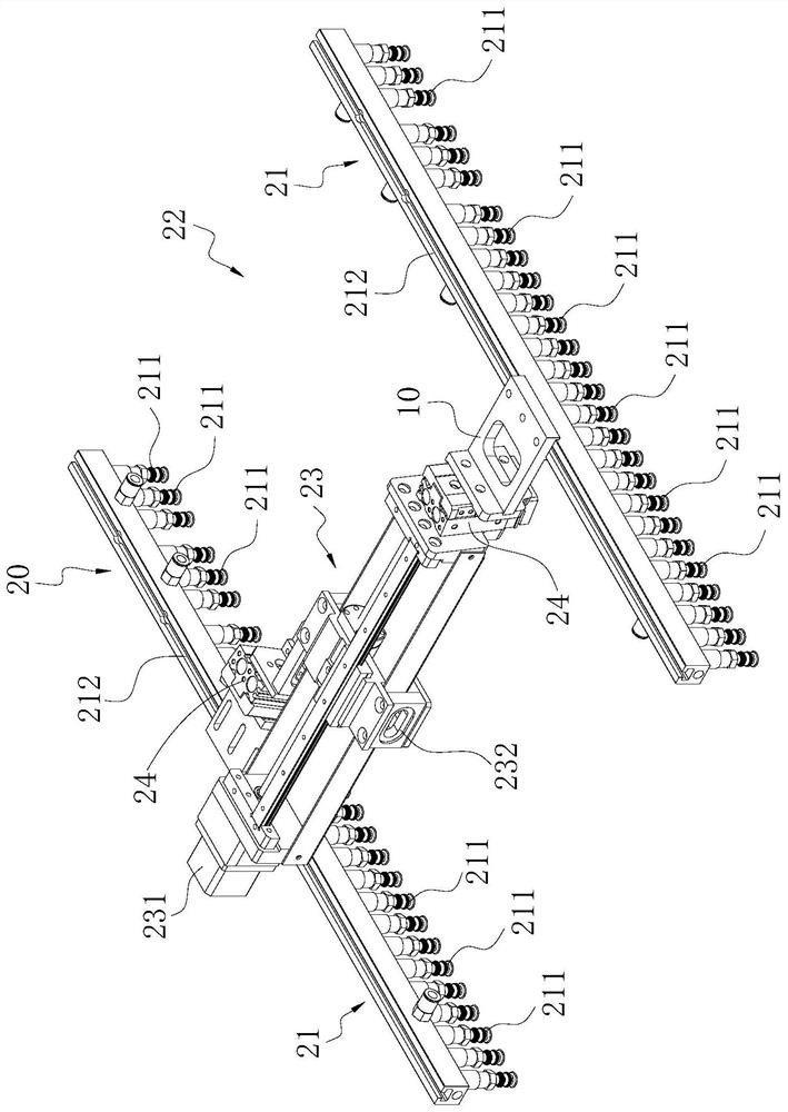
[0051] Embodiments of the present invention are described in detail below, examples of which are shown in the drawings, wherein the same or similar reference numerals designate the same or similar elements or elements having the same or similar functions throughout. Attached below by reference Figure 1-11 The described embodiments are exemplary and are intended to explain the present invention, but should not be construed as limiting the present invention.

[0052] In describing the present invention, it should be understood that the terms "length", "width", "upper", "lower", "front", "rear", "left", "right", "vertical", The orientation or positional relationship indicated by "horizontal", "top", "bottom", "inner", "outer", etc. are based on the orientation or positional relationship shown in the drawings, and are only for the convenience of describing the present invention and simplifying the description, rather than Nothing indicating or implying that a referenced device o...


PUM


Abstract

The invention belongs to the technical field of circuit board production equipment, and particularly relates to a PCB (Printed Circuit Board) picking and placing device and a PCB position correcting method. The PCB picking and placing device comprises a mounting frame, a picking and placing mechanism and a position recognizing mechanism, wherein the mounting frame is provided with a mounting position for mounting an external mechanical arm; the picking and placing mechanism is mounted on the mounting frame and is provided with a picking and placing area; the picking and placing area is used for sucking or placing a PCB; and the position recognizing mechanism is mounted on the mounting frame and located in the picking and placing area and is used for recognizing the deviation position of the edge of the PCB. If the PCB has a deviation condition, the mechanical arm drives the mounting frame to rotate and/or move at the moment, and the purpose of correcting the position of the PCB and then placing the PCB on another process to achieve transfer is achieved, so that the deviation position of the PCB is corrected in the PCB transfer process, damage to the PCB is avoided in the correcting process, and the transfer efficiency of the PCB is effectively improved. In addition, the mode is also suitable for relatively thin PCBs.

Description

technical field [0001] The invention belongs to the technical field of circuit board production equipment, and in particular relates to a PCB board pick-and-place device and a PCB board position correction method. Background technique [0002] In the PCB board manufacturing process of the electronics industry, it is necessary to pick up and place the stacked PCB boards on the board machine in the board board box on the conveyor belt to enter the main process line. In actual situations, there will be PCB boards in the stacked PCB boards. Stacking misalignment, that is, the problem of uneven stacking, then when picking and placing the PCB board, it is necessary to correct the offset PCB board and place it on the main process line for transportation; or it is necessary to stack the PCB boards flowing from the main process line At this time, some PCB boards flowing from the main process line will also be relatively offset. In the prior art, the commonly used method is to set to...

Claims


Application Information

Patent Timeline
Patent Type & Authority Applications(China)
IPC IPC(8): B65G49/06
CPCB65G49/061
Inventor 徐冬冬石智力刘文彪李巍
Owner 深圳市创新特科技有限公司
Why Eureka
Try Eureka