GaN device structure and preparation method thereof

A device structure and device technology, applied in the field of GaN device structure and its preparation, can solve the problems of difficult effective control, complex process, limited switching, etc., and achieve the effect of fast switching speed and cost reduction

Inactive Publication Date: 2021-06-29
ZHEJIANG UNIV
View PDF7 Cites 0 Cited by
  • Summary
  • Abstract
  • Description
  • Claims
  • Application Information

AI Technical Summary

Problems solved by technology

[0005] In view of the above-mentioned shortcomings of the prior art, the purpose of the present invention is to provide a GaN device structure and its preparation method, which are used to solve the limitations of the normally-on depletion-type GaN device in the prior art, the difficulty of effective control of the switch, and the complexity of the process. question

Method used


Image

  • GaN device structure and preparation method thereof
  • GaN device structure and preparation method thereof
  • GaN device structure and preparation method thereof

Examples


Embodiment Construction

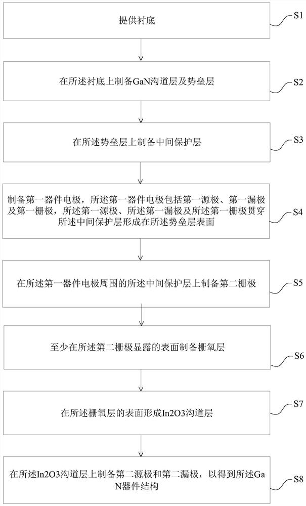
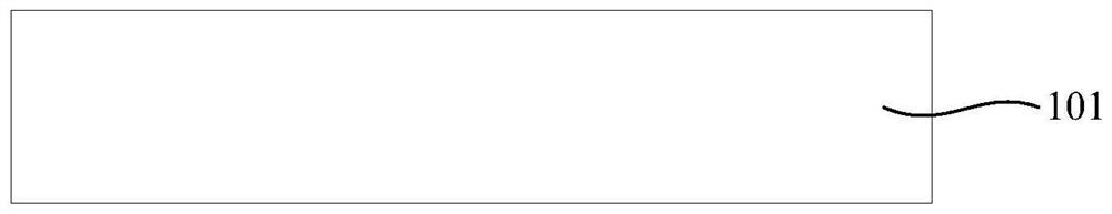
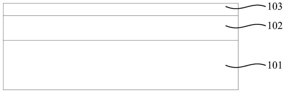
[0057] Embodiments of the present invention are described below through specific examples, and those skilled in the art can easily understand other advantages and effects of the present invention from the content disclosed in this specification. The present invention can also be implemented or applied through other different specific implementation modes, and various modifications or changes can be made to the details in this specification based on different viewpoints and applications without departing from the spirit of the present invention.

[0058]For example, when describing the embodiments of the present invention in detail, for the convenience of explanation, the cross-sectional view showing the device structure will not be partially enlarged according to the general scale, and the schematic diagram is only an example, which should not limit the protection scope of the present invention. In addition, the three-dimensional space dimensions of length, width and depth shou...


PUM

PropertyMeasurementUnit
thicknessaaaaaaaaaa
thicknessaaaaaaaaaa
thicknessaaaaaaaaaa

Abstract

The invention relates to a GaN device structure and a preparation method thereof. The preparation method comprises the following steps of: providing a substrate; preparing a GaN channel layer, a barrier layer, a middle protection layer and a first device electrode; preparing a second grid electrode on the middle protection layer around the first device electrode; and preparing a gate oxide layer, an In2O3 channel layer, a second source electrode and a second drain electrode. On the basis of a GaN device, an In2O3 device is introduced, and a normally-open depletion type GaN device is controlled to be turned on by using an In2O3MOSFET device, so that the limitation of a GaN normally-open type device is solved, and a normally-off function is realized; in addition, the problem that the process of connecting a Si device for switching control is complex is solved, the cost is reduced, compared with a SiMOSFET, the In2O3MOSFET is compatible with the subsequent process, that is, no complex technological process is needed, after the previous process of the GaN device process is completed, several steps of non-high-temperature processes are additionally added, the process can be completed, and the switching speed is high.

Description

technical field [0001] The invention belongs to the technical field of integrated circuit manufacturing, and in particular relates to a GaN device structure and a preparation method thereof. Background technique [0002] The research and application of GaN materials is the frontier and hotspot of global semiconductor research at present. It is a new type of semiconductor material for the development of microelectronic devices and optoelectronic devices. The third generation of semiconductor materials after semiconductor materials. It has properties such as wide direct band gap, strong atomic bond, high thermal conductivity, good chemical stability (hardly corroded by any acid) and strong radiation resistance. [0003] However, for a normally-on depletion-mode GaN device, that is, when the gate is at zero gate voltage, the channel is also turned on, and an additional negative gate voltage is required to turn off the channel, and the threshold voltage is negative. Obviously, ...

Claims


Application Information

Patent Timeline
Patent Type & Authority Applications(China)
IPC IPC(8): H01L21/82H01L27/06H01L29/78H01L29/24
CPCH01L21/82H01L27/0605H01L27/0617H01L29/78H01L29/24
Inventor 莫炯炯郁发新王志宇
Owner ZHEJIANG UNIV
Why Eureka
Try Eureka