Unlock instant, AI-driven research and patent intelligence for your innovation.

Preparation method of display substrate, display substrate and display device

A technology for display substrates and substrate substrates, which is used in identification devices, semiconductor/solid-state device manufacturing, instruments, etc., to avoid poor display, prevent serious metal oxidation, and improve product yield.

Pending Publication Date: 2021-07-02
HEFEI BOE DISPLAY TECH CO LTD +1
View PDF5 Cites 0 Cited by
  • Summary
  • Abstract
  • Description
  • Claims
  • Application Information

AI Technical Summary

Problems solved by technology

[0003] Embodiments of the present disclosure provide a method for preparing a display substrate, a display substrate, and a display device, so as to solve or alleviate one or more technical problems in the prior art

Method used


Image

  • Preparation method of display substrate, display substrate and display device
  • Preparation method of display substrate, display substrate and display device
  • Preparation method of display substrate, display substrate and display device

Examples


preparation example Construction

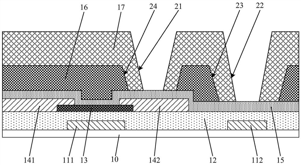
[0060] image 3 It is a schematic flow chart showing a method for preparing a substrate in an embodiment of the present disclosure. As shown in Figure 1, the method for preparing the display substrate may include:

[0061] S11, forming a thin film transistor structure on one side of the base substrate, the thin film transistor structure may include a gate metal layer, a first insulating layer, and a source-drain metal layer stacked in sequence;

[0062] S12, forming a second insulating layer on the side of the thin film transistor structure away from the substrate;

[0063] S13. Form a color-resistive layer and a third insulating layer in sequence on the side of the second insulating layer away from the base substrate, the third insulating layer is provided with a first via hole and a second via hole, and the first via hole is on the base substrate The orthographic projection of the source-drain metal layer at least partially intersects the orthographic projection of the sou...


PUM

PropertyMeasurementUnit
Thicknessaaaaaaaaaa
Thicknessaaaaaaaaaa
Thicknessaaaaaaaaaa

Abstract

The embodiment of the invention provides a preparation method of a display substrate. The preparation method comprises the steps that a second insulating layer is formed on the side, away from a substrate, of a thin film transistor structure; a color resistance layer and a third insulating layer are sequentially formed on the side, away from the substrate, of the second insulating layer, a first via hole and a second via hole are formed in the third insulating layer, and the orthographic projection of the first via hole on the substrate at least partially intersects with the orthographic projection of the source-drain metal layer on the substrate; a color resistance layer and / or a third insulating layer are / is reserved between the first via hole and the second insulating layer, and the second via hole exposes the second insulating layer; and the first via hole position and the second via hole position are etched by adopting an etching process, at least part of the source-drain metal layer is exposed at the first via hole position, and at least part of the gate metal layer is exposed at the second via hole position. According to the technical scheme, the metal at the first via hole position can be prevented from being exposed too early, the metal at the first via hole position is prevented from being seriously oxidized, and poor display of a product is avoided.

Description

technical field [0001] The present disclosure relates to the field of display technology, and in particular to a method for preparing a display substrate, a display substrate and a display device. Background technique [0002] In the process of preparing the color resist layer on the array substrate, the metal at the bottom of the pixel via hole is seriously oxidized, resulting in an increase in the contact resistance between the pixel electrode and the drain electrode, resulting in poor display. Contents of the invention [0003] Embodiments of the present disclosure provide a method for preparing a display substrate, a display substrate, and a display device, so as to solve or alleviate one or more technical problems in the prior art. [0004] As a first aspect of the embodiments of the present disclosure, the embodiments of the present disclosure provide a display substrate, including: [0005] Substrate substrate; [0006] A thin film transistor structure, located on...

Claims


Application Information

Patent Timeline
IPC IPC(8): H01L27/12H01L21/84G09F9/30
CPCH01L27/1218H01L27/1262H01L27/124H01L27/1248H01L27/1259G09F9/30H01L21/31116H01L21/31138
Inventor 陈亮高锦成钱海蛟姜涛刘泽旭汪涛赵立星张冠永柳泉洲刘建涛
Owner HEFEI BOE DISPLAY TECH CO LTD