Method and system for detecting wafer distribution range and storage medium

A distribution range and wafer technology, applied in the field of wafer bonding, can solve the problems of wafer waste, high time cost, etc., achieve the effect of reducing the search area and improving work efficiency

Active Publication Date: 2021-07-09
SHEN ZHEN TALUER TECH CO LTD
View PDF8 Cites 0 Cited by
  • Summary
  • Abstract
  • Description
  • Claims
  • Application Information

AI Technical Summary

Problems solved by technology

In order to get it clean, you can only check it in all possible places, so that more than half of the time is running empty, and the time cost is too high; and for efficiency, selectively skip blank positions, so that those island areas will be skipped Not taking it will cause a waste of wafers, which is also unacceptable to all manufacturers

Method used


Image

  • Method and system for detecting wafer distribution range and storage medium
  • Method and system for detecting wafer distribution range and storage medium

Examples


Embodiment Construction

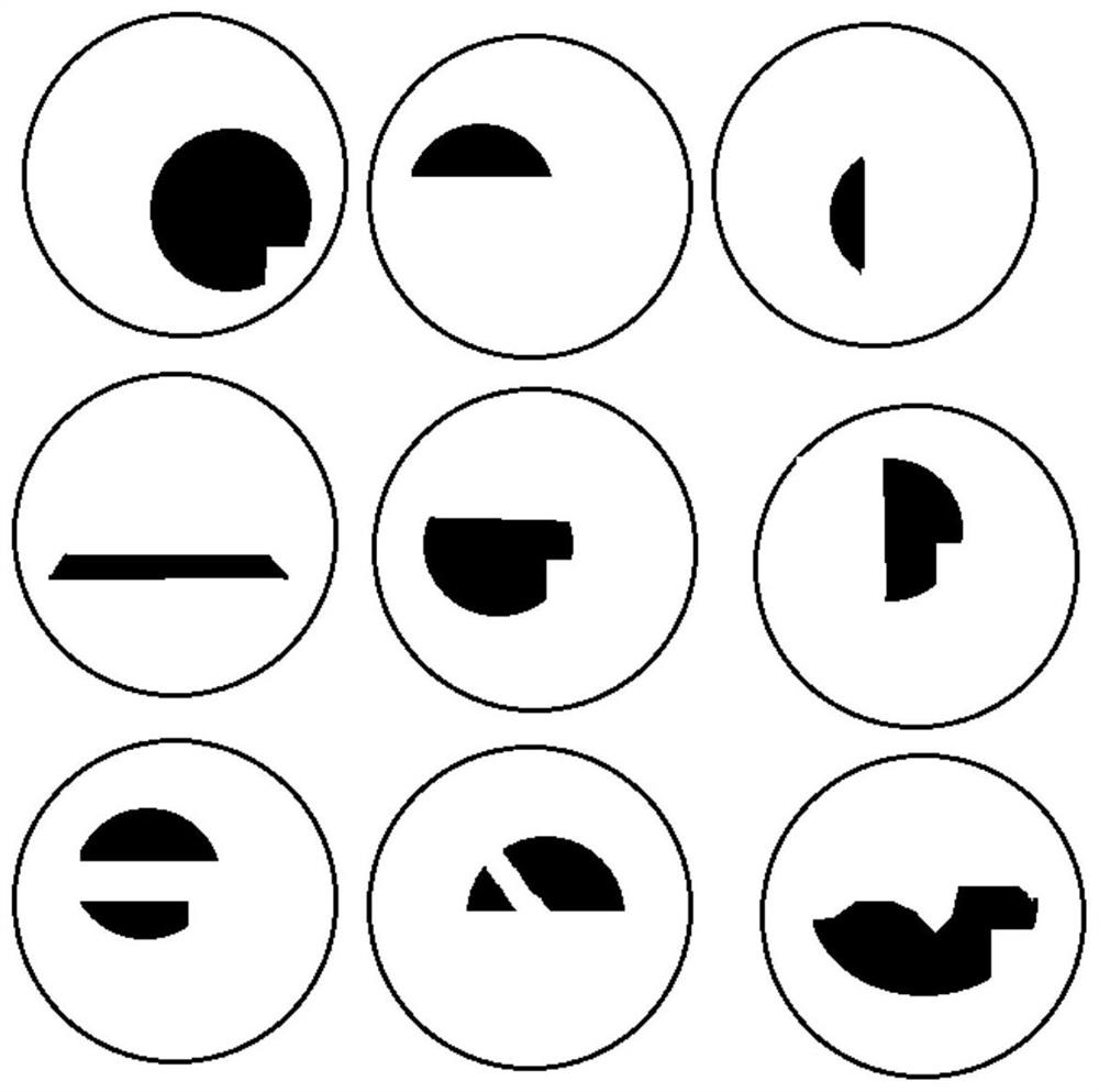
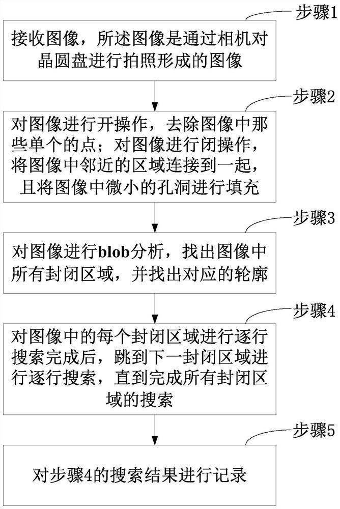
[0027] First of all, let's take a look at the wafer distribution diagram, such as figure 1 As shown, the distribution range of wafers from upstream is various, especially the wafers left after trial production or production of die bonders from multiple manufacturers. figure 1 The circle in represents the inner frame of the wafer disk, and it can be seen that the wafer distribution is uncertain.

[0028] In the present invention, a camera is added, and the camera is preferably a global camera. Specifically, a global camera is added at an appropriate position of the device, and after the orientation of the wafer is correct, a photo is taken of the entire wafer. In order to reduce distortion and take into account the installation position, a medium focal length or a slightly longer lens can be used. Generally, the distortion can reach less than 0.5%. The calibration template produced by the camera manufacturer can also be used to calibrate the image, and relevant information can...


PUM


Abstract

The invention provides a method and system for detecting a wafer distribution range and a storage medium. The method comprises steps of 1, a data receiving step, receiving an image which is an image formed by photographing a wafer disc through a camera; 2, an image processing step, carrying out opening operation on the image, and removing single points in the image; performing closing operation on the image, and connecting adjacent areas in the image together; step 3, an image analysis step, finding out all closed areas in the image, and finding out corresponding contours; step 4, a searching step, after the line-by-line searching of the first closed area in the image is completed, jumping to the next closed area to perform the line-by-line searching till the searching of all closed areas is completed; and 5, recording, recording the search result in the step 4. The method is advantaged in that discontinuous closed areas can be quickly traversed without duplication or missing, and blank areas can be directly skipped without detection, so search areas are greatly reduced, and working efficiency is improved.

Description

technical field [0001] The invention relates to the technical field of wafer bonding, in particular to a method, system and storage medium for detecting the distribution range of wafers. Background technique [0002] In the die-bonding equipment, there is an essential premise that the precise position of each wafer in the wafer tray must be known before the next step can be performed. During the process of expanding the wafer, the overall wafer will be shifted, and the relative position between the wafers will change randomly. Currently, machine vision is used to adapt to this situation. [0003] As the wafers are getting smaller and smaller, in order to ensure the accuracy, only about 30 or less can be taken each time, and only the most central one is taken each time, while there are tens of thousands of wafers in a whole plate. In order to get it clean, you can only check it in all possible places, so that more than half of the time is running empty, and the time cost is ...

Claims


Application Information

Patent Timeline
Patent Type & Authority Applications(China)
IPC IPC(8): G01N21/95G01N21/01
CPCG01N21/9505G01N21/01G01N2021/0112
Inventor 马春平曾逸刘耀金
Owner SHEN ZHEN TALUER TECH CO LTD
Why Eureka
Try Eureka