
Manufacturing method of copper block-embedded circuit board

A manufacturing method and technology of embedding copper blocks, which are applied in the fields of printed circuit manufacturing, printed circuits, electrical components, etc., can solve the problems such as difficulty in clearing glue on buried copper block circuit boards, etc.

Active Publication Date: 2021-07-30
DONGGUAN SHENGYI ELECTRONICS
View PDF5 Cites 0 Cited by
  • Summary
  • Abstract
  • Description
  • Claims
  • Application Information

AI Technical Summary

Problems solved by technology

[0004] The purpose of the present invention is to provide a method for making a buried copper circuit board, which can solve the problem that the residual glue on the surface of the buried copper circuit board is not easy to remove, so as to improve the glue removal efficiency

Method used


Image

  • Manufacturing method of copper block-embedded circuit board

Examples


Embodiment Construction

[0031] In order to make the purpose, technical solutions and advantages of the embodiments of the present invention clearer, the technical solutions in the embodiments of the present invention will be clearly and completely described below in conjunction with the drawings in the embodiments of the present invention. Obviously, the described embodiments It is a part of embodiments of the present invention, but not all embodiments. The components of the embodiments of the invention generally described and illustrated in the figures herein may be arranged and designed in a variety of different configurations.

[0032] Accordingly, the following detailed description of the embodiments of the invention provided in the accompanying drawings is not intended to limit the scope of the claimed invention, but merely represents selected embodiments of the invention. Based on the embodiments of the present invention, all other embodiments obtained by persons of ordinary skill in the art wi...


PUM


Abstract

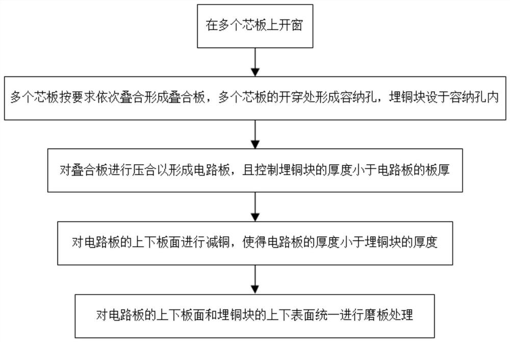
The invention discloses a manufacturing method of a copper-block-embedded circuit board, and relates to the technical field of printed circuit board manufacturing. The thickness of the embedded copper block is controlled to be smaller than that of the circuit board, the height difference prevents glue from flowing to the board surface of the circuit board after lamination, and the phenomenon of residual glue on the board surface is avoided; copper reduction treatment is carried out on the upper and lower surfaces of the circuit board, so that the thickness of the circuit board is smaller than that of the embedded copper block, and the height difference enables the upper and lower surfaces of the embedded copper block to protrude out of the circuit board, so that the upper and lower surfaces of the embedded copper block are subjected to glue removal; finally, the upper and lower board surfaces of the circuit board and the upper and lower surfaces of the embedded copper block are subjected to board grinding treatment to remove colloid on the upper and lower surfaces of the embedded copper block, and meanwhile it is guaranteed that the upper and lower board surfaces of the circuit board are flush with the upper and lower surfaces of the embedded copper block. According to the manufacturing method, the glue removing efficiency is improved, and meanwhile, the board surface of the copper block embedded circuit board is prevented from being deformed and damaged.

Description

technical field [0001] The invention relates to the technical field of manufacturing printed circuit boards, in particular to a method for manufacturing printed circuit boards with buried copper blocks. Background technique [0002] Nowadays, embedded copper blocks are generally arranged in the circuit board to ensure good heat dissipation of the circuit board. During the production process of the buried copper block circuit board, it is necessary to use colloid to connect the buried copper block and the circuit board. However, during the pressing process of the circuit board, the colloid is easy to overflow and flow to the board surface and the buried copper block, thus making the buried copper block There are different degrees of residual glue on the surface of each circuit board. [0003] There is a method for making a buried copper circuit board, which controls the thickness of the buried copper block to be greater than the actual board thickness after lamination, so th...

Claims


Application Information

Patent Timeline
IPC IPC(8): H05K3/40
CPCH05K3/4007
Inventor 何思良宋祥群刘梦茹杨云
Owner DONGGUAN SHENGYI ELECTRONICS
Learn More