
Laser spot position correction method and chip scale wafer level marking equipment

A correction method and laser spot technology, applied in the field of laser marking, can solve the problems of slow speed, low efficiency and low positioning accuracy, and achieve the effect of ensuring accuracy

Active Publication Date: 2021-08-13
SUZHOU SECOTE PRECISION ELECTRONICS CO LTD
View PDF5 Cites 0 Cited by
  • Summary
  • Abstract
  • Description
  • Claims
  • Application Information

AI Technical Summary

Problems solved by technology

[0005] In view of this, an embodiment of the present invention provides a laser spot position correction method and a chip-scale wafer-level marking device to solve the problems of low positioning accuracy, low efficiency and slow speed in the traditional mechanical positioning method of the laser marking device

Method used


Image

  • Laser spot position correction method and chip scale wafer level marking equipment
  • Laser spot position correction method and chip scale wafer level marking equipment
  • Laser spot position correction method and chip scale wafer level marking equipment

Examples


Embodiment 1

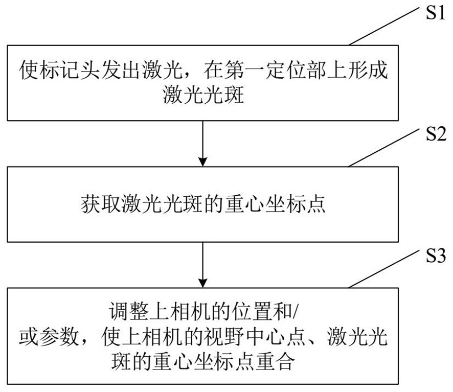
[0042] An embodiment of the present invention provides a laser spot position correction method, such as figure 1 shown, including:

[0043] In step S1, the marking head emits laser light to form a laser spot on the first positioning part. The first positioning part is fixed on the placing table.

[0044] In this embodiment, the marking head is controlled to emit laser light toward the center of the first positioning portion. Specifically, the first positioning part is glass coated with white paint, which prevents the laser light from directly hitting the camera lens through the glass.

[0045] In this embodiment, the method enlarges the laser spot through computer vision, and calculates the laser energy center through an algorithm, so as to eliminate the position deviation caused by laser irregularity.

[0046] Step S2, acquiring the barycenter coordinate point of the laser spot.

[0047] In this embodiment, since the laser spot is very small, at the micron level, the corr...

Embodiment 2

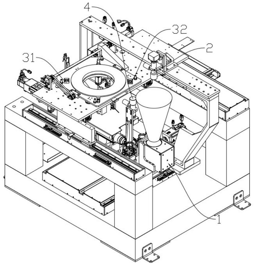
[0066] An embodiment of the present invention provides a chip-scale wafer-level marking device, using the method for correcting the laser spot position in the above-mentioned embodiment, such as image 3 As shown, it includes: a marking head 1, an upper camera 2, a first positioning part 31 and a lower camera 4, wherein: the upper camera 2 is fixed on the mounting plate through the first bracket, and the upper camera 2 is located above the placement table and faces the placement The upper end surface of the platform; the X-axis translation assembly is connected with the placement platform, and the X-axis translation assembly is used to drive the placement platform to move along the X-axis; the lower camera 4 is fixed on the mounting plate through the second bracket , the lower camera 4 is located below the placement platform and faces the lower end surface of the placement platform; the first positioning part 31 is arranged on the placement platform; the marking head 1 is fixed...


PUM


Abstract

The invention discloses a laser spot position correction method and chip scale wafer level marking equipment. The method comprises the steps that a marking head is made to emit laser, and a laser spot is formed on a first positioning part; the first positioning part is fixed on a containing table; a barycentric coordinate point of the laser spot is acquired; and parameters of an upper camera are adjusted to enable the lens center point of the upper camera to coincide with the barycentric coordinate point of the laser spot, wherein the marking head is fixed in a laser marking device, and the upper camera is fixed above the first positioning part, and a lens of the upper camera faces the first positioning part. According to the method, after the parameters are set by the marking head, a laser beam is emitted to the first positioning part, the light spot is formed on the first positioning part, the upper camera shoots the light spot, a laser spot image is obtained, the view center point of the laser spot image shot by the upper camera coincides with the barycentric coordinate point of the laser spot by adjusting the parameters of the upper camera, camera compensation is achieved, and therefore the precision of the marking head is ensured.

Description

technical field [0001] The invention relates to the technical field of laser marking, in particular to a laser spot position correction method and chip-scale wafer-level marking equipment. Background technique [0002] Wafer marking is to use high-energy-density laser beams to irradiate the surface of the wafer locally, so that the surface material rapidly vaporizes or undergoes a color change, thereby exposing deep-layer substances, or engraving traces by chemically and physically changing the surface materials, or through light energy. Burn off part of the material to reveal the graphics and text to be etched. [0003] In the prior art, traditional mechanical positioning methods are mostly used. When analyzing workpiece positioning schemes, the concept of positioning support points, that is, the "six-point rule", is usually used. When the workpiece is actually positioned in the fixture, this theoretical "point" is not used to contact the positioning reference plane of the...

Claims


Application Information

Patent Timeline
IPC IPC(8): B23K26/362B23K26/03H01L21/67H01L21/68
CPCB23K26/032B23K26/362H01L21/67282H01L21/681
Inventor 孙丰张宝峰吴斌刘斌
Owner SUZHOU SECOTE PRECISION ELECTRONICS CO LTD
Learn More