Segmentation and verification method, device, electronic device, storage medium

A chip design and classification information technology, applied in CAD circuit design, special data processing applications, etc., can solve the problems of system performance degradation, failure to accurately reflect the performance and functions of the original chip design, and achieve the effect of offsetting the effect of delay

Active Publication Date: 2021-10-01
S2C
View PDF11 Cites 0 Cited by
  • Summary
  • Abstract
  • Description
  • Claims
  • Application Information

AI Technical Summary

Problems solved by technology

[0003] In the partition verification of chip design, because the time delay of the interconnection signal transmission between FPGAs is usually much greater than the time delay of the internal signal transmission of the FPGA, when performing partition verification in a multi-FPGA prototype verification system, it is possible to introduce many factors. New problems that do not exist in the design, and new solutions are required to solve these new problems, and there may be other new problems in the new solutions to solve new problems, such as system performance degradation, verification does not accurately reflect the original chip design performance and function

Method used


Image

  • Segmentation and verification method, device, electronic device, storage medium
  • Segmentation and verification method, device, electronic device, storage medium
  • Segmentation and verification method, device, electronic device, storage medium

Examples


example 1

[0080] Example 1, such as Figure 6 As shown, the boundary cut2 can be adjusted to the output line of the sequential logic circuit g0. Correspondingly, the data conditions of the receiving end and the sending end on both sides of the boundary before and after the division can be as follows Figure 7 shown.

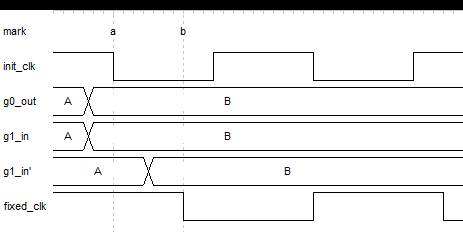
[0081] Before cutting, the sequential logic circuit can receive and send data correctly under the action of the clock init_clk, such as sending data on the rising edge of the clock and receiving data on the falling edge, such as the data sent by the sequential logic circuit g0 (such as data C0, D0, E0, etc., see the g0_out icon in the figure), g1 normally receives the data (see the g1_in icon in the figure), correspondingly, g1 obtains the corresponding output data after processing (such as data C1, D1, E1, etc., see the figure g1_out in the diagram), and the sequential logic circuit g2 can receive the data output by g1 in time (such as data C1, D1, E1, etc., see the g2_i...

example 2

[0083] Example 2, such as Figure 8 As shown, the division boundary can be adjusted between the two sequential logic circuits, for example, the boundary can be adjusted to the output line of the sequential logic circuit g0, and TDM can be inserted there to solve the IO requirements in the verification; correspondingly, the division before and after The data situation of the receiving end and the sending end on both sides of the boundary can be as follows Figure 9 shown.

[0084] Assuming that the clock frequency of the TDM sampling is consistent with the originally designed clock frequency clk, there may be a stable time difference between the data received by the receiving end of the TDM and the data sent by the sending end (as shown in the figure between mark b and mark c time difference), when the data of the receiving end g1 passes through the time interval between receiving data on the falling edge of the sequential logic circuit and sending data on the rising edge, for...


PUM


Abstract

The implementation of this specification provides a segmentation and verification method, device, electronic equipment, and storage medium, which are applied in the field of electronic design automation technology. The segmentation scheme includes: classifying the nodes in the chip design, and merging the classified nodes Processing, splitting the merged new node, so as to set the split boundary on the link driven by the trigger. The accuracy and efficiency of chip design segmentation and verification can be improved by optimally adjusting all segmentation boundaries to the wires with flip-flop drives.

Description

technical field [0001] This specification relates to the technical field of electronic design automation, and in particular to a segmentation and verification method, device, electronic equipment, and storage medium for chip design segmentation verification. Background technique [0002] At present, a chip design is usually divided into multiple code blocks (that is, partitions), and multiple verification chips (such as FPGA, field programmable gate array) are used to form a prototype verification system (such as a multi-FPGA prototype verification system). verify. [0003] In the partition verification of chip design, because the time delay of the interconnection signal transmission between FPGAs is usually much greater than the time delay of the internal signal transmission of the FPGA, when performing partition verification in a multi-FPGA prototype verification system, it is possible to introduce many factors. New problems that do not exist in the design, and new soluti...

Claims


Application Information

Patent Timeline
Patent Type & Authority Patents(China)
IPC IPC(8): G06F30/34
CPCG06F30/34
Inventor 万鹭张吉锋肖慧邵中尉
Owner S2C
Why Eureka
Try Eureka