Semiconductor packaging device and manufacturing method thereof

A technology of packaging device and manufacturing method, which is applied in semiconductor/solid-state device manufacturing, semiconductor devices, semiconductor/solid-state device components, etc., can solve the problems of large packaging volume and poor heat dissipation performance, and achieve improved recognition sensitivity and accuracy and sensitivity, the effect of improving flexibility

Active Publication Date: 2021-08-13
江苏华昶熠电子科技有限公司
View PDF4 Cites 2 Cited by
  • Summary
  • Abstract
  • Description
  • Claims
  • Application Information

AI Technical Summary

Problems solved by technology

However, in the existing semiconductor package, there are disadvantages such as large package volume and poor heat dissipation performance.

Method used


Image

  • Semiconductor packaging device and manufacturing method thereof
  • Semiconductor packaging device and manufacturing method thereof
  • Semiconductor packaging device and manufacturing method thereof

Examples


Embodiment Construction

[0026] In order to better understand the technical solutions of the present invention, the embodiments of the present invention will be described in detail below in conjunction with the accompanying drawings.

[0027] It should be clear that the described embodiments are only some of the embodiments of the present invention, not all of them. Based on the embodiments of the present invention, all other embodiments obtained by persons of ordinary skill in the art without creative efforts fall within the protection scope of the present invention.

[0028] The present invention proposes a manufacturing method of a semiconductor packaging device, the manufacturing method of the semiconductor packaging device includes the following steps:

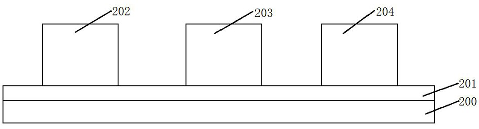
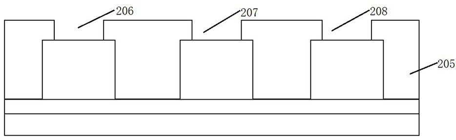
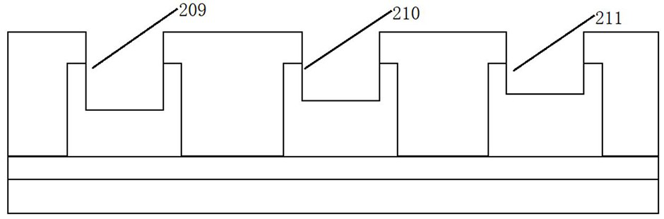
[0029] (1) First, a carrier substrate is provided, and a first rewiring layer is formed on the carrier substrate, and then a first semiconductor chip, a second semiconductor chip, and a third semiconductor chip are arranged at intervals on the fi...


PUM


Abstract

The invention relates to a semiconductor packaging device and a manufacturing method thereof. A first trench, a second trench and a third trench are respectively formed on the back surfaces of a first semiconductor chip, a second semiconductor chip and a third semiconductor chip, so that the depth of the first trench is larger than that of the second trench, the depth of the second trench is larger than that of the third trench, and a fourth semiconductor chip, a fifth semiconductor chip and a sixth semiconductor chip are arranged in the first trench, second and third trenches. By means of the structure, the height difference of the active faces of the semiconductor chips can be effectively adjusted, and the semiconductor packaging flexibility is further improved; when the fourth semiconductor chip is a light-emitting chip, the fifth semiconductor chip is a light sensing chip, and when the sixth semiconductor chip is a biological recognition chip, the recognition sensitivity of the light sensing chip can be effectively improved, and the accuracy and sensitivity of biological recognition are improved.

Description

technical field [0001] The invention relates to the field of semiconductor packaging, in particular to a method for manufacturing a semiconductor packaging device. Background technique [0002] In an existing semiconductor packaging device, a semiconductor chip is usually placed on a printed circuit board through a wire bonding process or a flip-chip welding process, and then a molding compound layer is provided to wrap the printed circuit board and the semiconductor chip. Conventional semiconductor packages include dual in-line packages, ball grid array packages, plastic quad flat packages, pin grid array packages, multi-die stack packages, and chip scale packages. Different chip types are packaged using different packaging technologies. However, existing semiconductor packages have disadvantages such as large package volume and poor heat dissipation performance. Contents of the invention [0003] The object of the present invention is to overcome the shortcomings of th...

Claims


Application Information

Patent Timeline
Patent Type & Authority Applications(China)
IPC IPC(8): H01L21/50H01L51/56H01L25/16H01L23/367H01L23/31
CPCH01L21/50H01L25/167H01L23/367H01L23/3107H10K71/00
Inventor 周华
Owner 江苏华昶熠电子科技有限公司
Why Eureka
Try Eureka