
Semiconductor device

a technology of semiconductor devices and semiconductors, applied in semiconductor devices, semiconductor/solid-state device details, electrical apparatus, etc., can solve the problem of hardly conveying tape smoothly, and achieve the effect of reducing manufacturing costs, improving fabrication effectiveness, and designing flexiblely

Inactive Publication Date: 2010-02-23
LAPIS SEMICON CO LTD
View PDF10 Cites 0 Cited by
  • Summary
  • Abstract
  • Description
  • Claims
  • Application Information

AI Technical Summary

Benefits of technology

The present invention provides a semiconductor package structure with improved flexibility, reliability, and ease of fabrication. The structure includes a base tape with roller-contact regions, no sprocket hole, and a protecting layer. The absence of sprocket holes allows for flexibility in package size design and reduces manufacturing costs. The base tape is also stronger at the edges. Overall, the invention simplifies the conveying process and improves the strength of the package.

Problems solved by technology

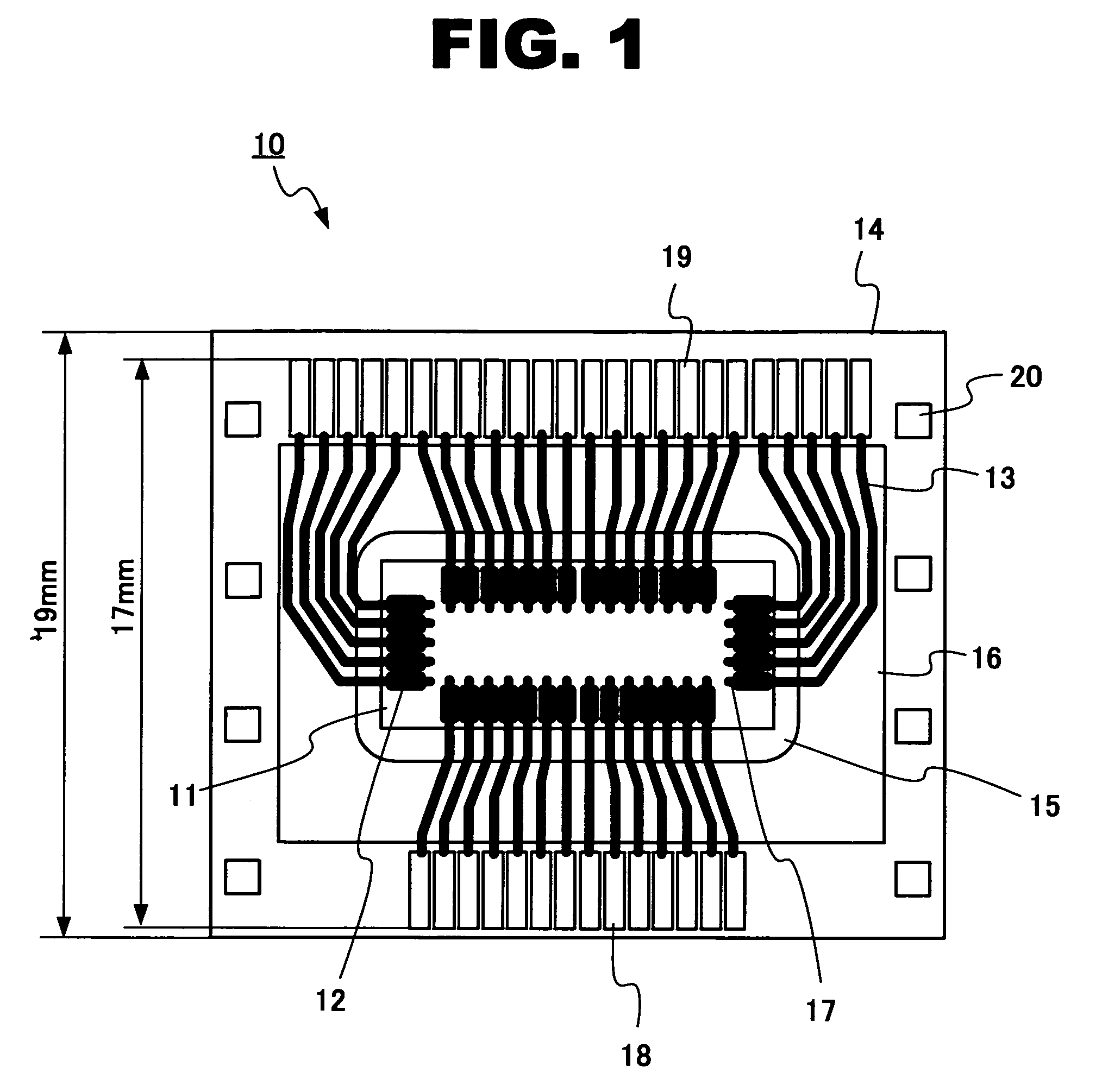
According to a structure shown in Patent Publication 1, since sprocket holes are provided at a region where a roller is to be in contact with, there were the following problems.(1) The strength of a tape is lowered by sprocket holes.(2) Unevenness over the sprocket holes makes vibration in a conveying process, and therefore, a tape is hardly conveyed smoothly.
Further, according to a structure shown in Patent Publication 2, the same or similar problems as the Patent Publication 1 arise.

Method used


Image

  • Semiconductor device
  • Semiconductor device
  • Semiconductor device

Examples


Embodiment Construction

[0039]In the following detailed description of the preferred embodiments, reference is made to the accompanying drawings which form a part hereof, and in which is shown by way of illustration specific preferred embodiments in which the inventions may be practiced. These preferred embodiments are described in sufficient detail to enable those skilled in the art to practice the invention, and it is to be understood that other preferred embodiments may be utilized and that logical, mechanical and electrical changes may be made without departing from the spirit and scope of the present inventions. The following detailed description is, therefore, not to be taken in a limiting sense, and scope of the present inventions is defined only by the appended claims.

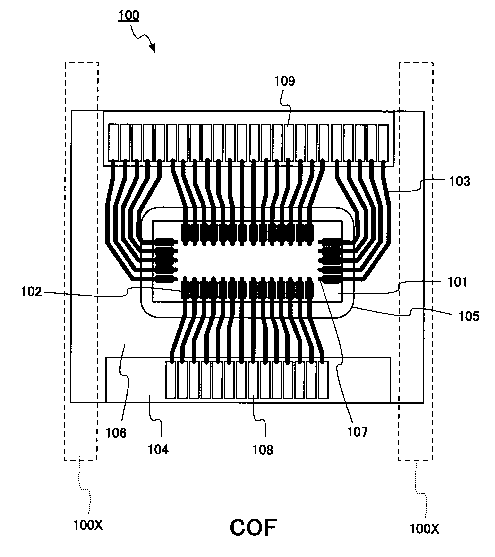
[0040]FIG. 3 is a plan view (perspective view) showing a COF package according to a first preferred embodiment of the present invention. FIG. 4 is a plan view showing COF packages shown in FIG. 3, which are mounted on a base tape. A s...


PUM


Abstract

A semiconductor device according to the present invention includes a base tape (film carrier tape); a semiconductor chip mounted on the base tape; conducting leads formed on the base tape to be connected to the semiconductor chip; input terminals and output terminals connected to the conducting leads; and a protecting layer formed to cover the conducting leads completely. The base tape is provided at its side edges with roller-contact regions, where carrier rollers are to be in contact with. No holes and no unevenness area is formed on the roller-contact regions.

Description

CROSS REFERENCE TO RELATED APPLICATION[0001]This application claims the priority of Application No. 2007-288026, filed Nov. 6, 2007 in Japan, the subject matter of which is incorporated herein by reference.TECHNICAL FIELD OF THE INVENTION[0002]The present invention relates to a semiconductor device fabricated using a tape-shaped base member. In more detail, the present invention relates to a semiconductor device (package) of a structure of COF (Chip On Film), TCP (Tape Carrier Package) or the like.BACKGROUND OF THE INVENTION[0003]According to TCP and COF using a tape-shaped base member, a semiconductor package is fabricated, for example, using a polyimide tape having a width of about 35 mm. A copper foil or a copper plating layer is formed on the polyimide tame to form an electric circuit thereon. According to a TCP type of semiconductor package, a polyimide tape is removed at an area for a semiconductor chip, and copper leads connected to the semiconductor chip are exposed, which i...

Claims


Application Information

Patent Timeline
Patent Type & Authority Patents(United States)
IPC IPC(8): H01L23/495
CPCH01L23/4985H01L23/49838H01L2924/0002H01L2924/00
Inventor TAKAHASHI, YOSHIKAZU
Owner LAPIS SEMICON CO LTD
Learn More