Supercharge Your Innovation With Domain-Expert AI Agents!

Inner-layer board high-vacuum continuous laminating device and method for PCB (Printed Circuit Board) circuit process

A pressing device and inner layer board technology, applied in lamination devices, lamination, chemical instruments and methods, etc., can solve the problems of low efficiency, long heating and cooling time, long waiting time for pressing, etc., and achieve continuous Pressing and improving the effect of pressing efficiency

Pending Publication Date: 2021-08-13
江西旭昇电子有限公司
View PDF9 Cites 0 Cited by
  • Summary
  • Abstract
  • Description
  • Claims
  • Application Information

AI Technical Summary

Problems solved by technology

The existing process has the following disadvantages: the heating and cooling time is long, the waiting time for pressing is long, and the efficiency is low

Method used


Image

  • Inner-layer board high-vacuum continuous laminating device and method for PCB (Printed Circuit Board) circuit process
  • Inner-layer board high-vacuum continuous laminating device and method for PCB (Printed Circuit Board) circuit process
  • Inner-layer board high-vacuum continuous laminating device and method for PCB (Printed Circuit Board) circuit process

Examples


Embodiment Construction

[0029] In order to enable those skilled in the art to better understand the technical solutions in the embodiments of the present invention, and to make the above-mentioned purpose, features and advantages of the present invention more obvious and understandable, the specific implementation of the present invention will be further described below in conjunction with the accompanying drawings illustrate.

[0030] It should be noted here that the descriptions of these embodiments are used to help understand the present invention, but are not intended to limit the present invention. In addition, the technical features involved in the various embodiments of the present invention described below may be combined with each other as long as they do not conflict with each other.

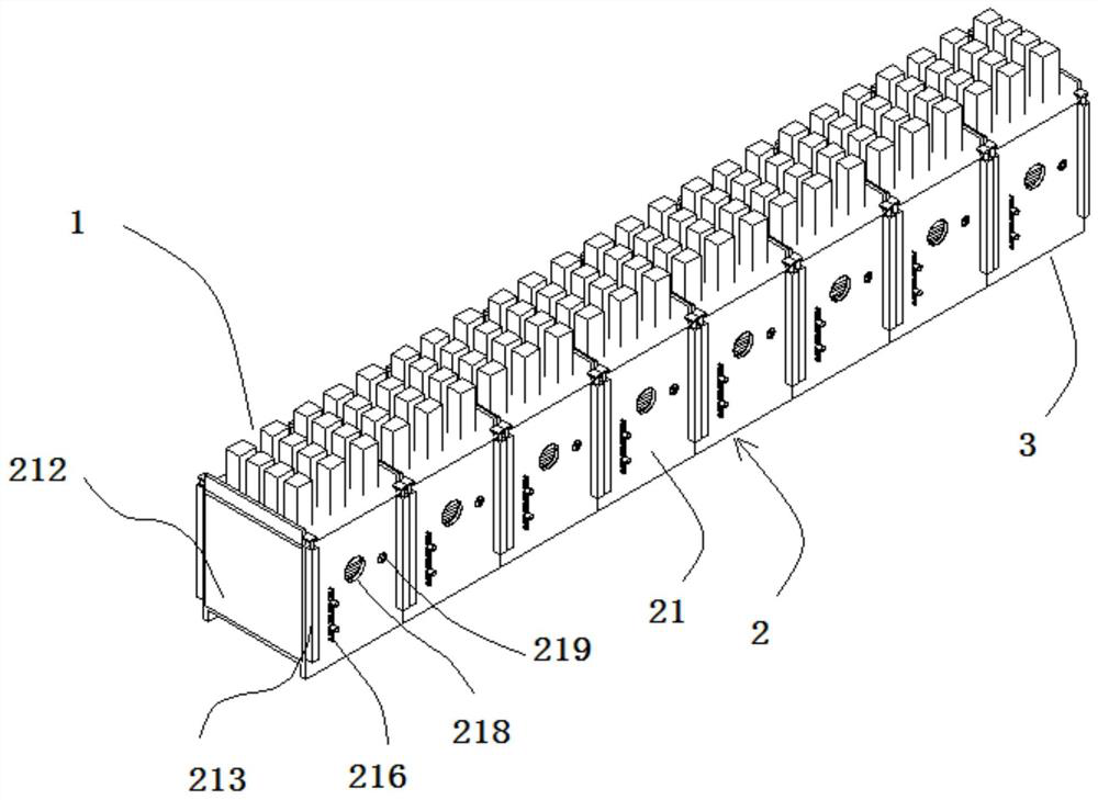
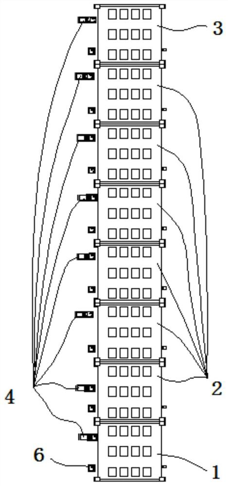
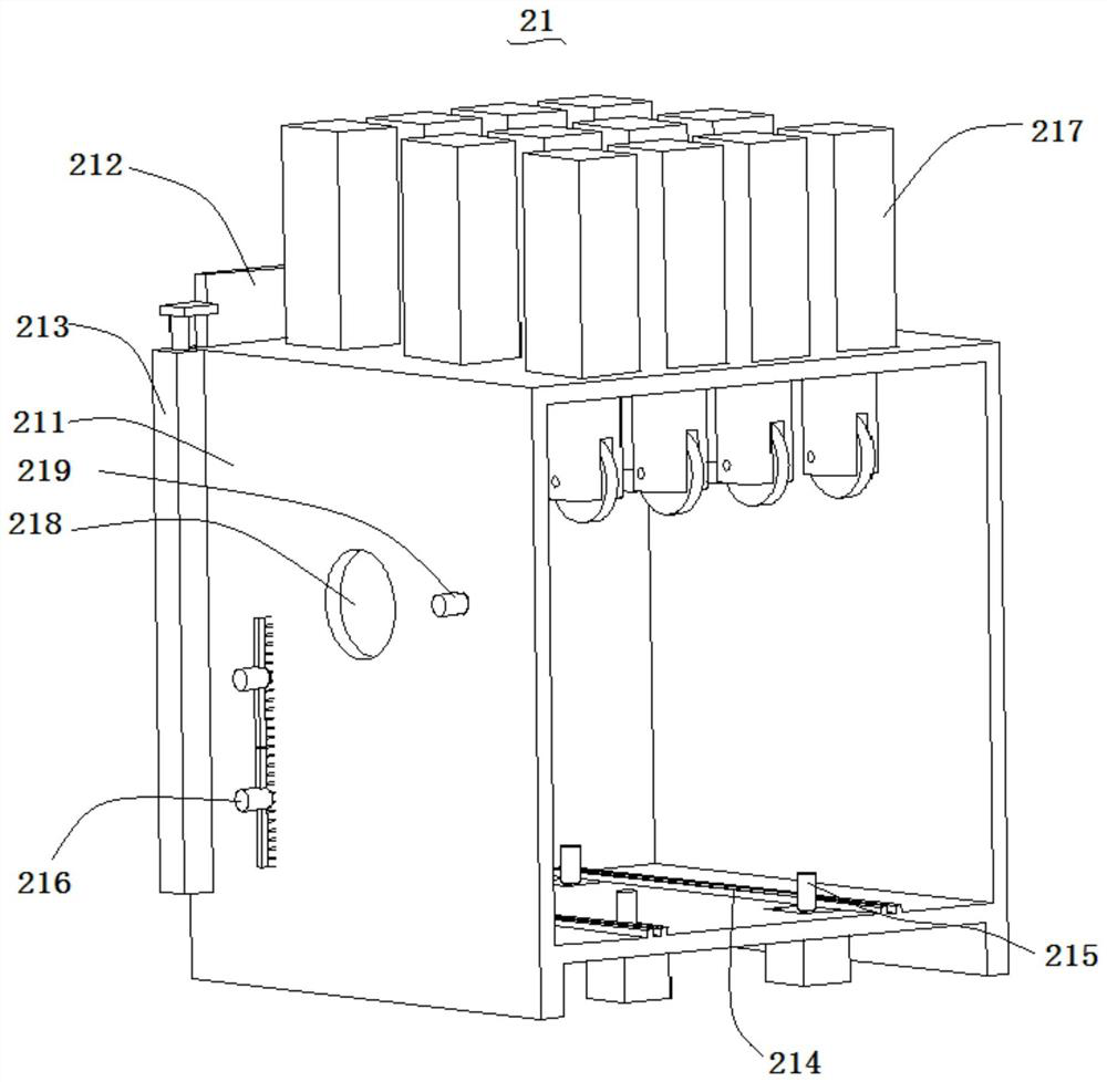
[0031] Please refer to figure 1 and figure 2 , figure 1 It is a schematic diagram of the high-vacuum continuous pressing device for the inner layer board of the PCB circuit technology provided by the pres...


PUM


Abstract

The invention discloses an inner-layer board high-vacuum continuous pressing device for a PCB (Printed Circuit Board) circuit process, which comprises a feeding bin, a continuous pressing bin and a discharging bin which are connected in sequence, as well as a vacuum pump unit and a display control device. A to-be-pressed board assembly is conveyed through a feeding and discharging trolley and sequentially passes through the feeding bin, the continuous pressing bin and the discharging bin till the pressing process is completed. The vacuum pump unit is connected with the feeding bin, the continuous pressing bin and the discharging bin. The interior of the continuous pressing bin is in a vacuum state during working, and the pressure states of the feeding bin and the discharging bin are adjusted according to corresponding working requirements. According to the inner-layer board high-vacuum continuous pressing device for the PCB circuit process, continuous pressing of the inner-layer board of the PCB circuit can be achieved, and the pressing efficiency is improved. Based on the pressing device, the invention further provides an inner-layer board high-vacuum continuous pressing method for the PCB circuit process.

Description

technical field [0001] The invention relates to the technical field of printed circuit board production, in particular to a high-vacuum continuous pressing device and method for inner layer boards of PCB circuit technology. Background technique [0002] The current laminating process of the inner layer of the PCB circuit board is: plate to be laminated->carrying plate->pressing (pressing number<=pressing machine capacity)->cooling->pressing completed. The existing technology has the following disadvantages: the time for heating and cooling is long, the time for waiting for pressing is long, and the efficiency is low. [0003] In view of this, it is necessary to provide a new inner layer lamination process of PCB circuit technology to solve the above technical problems. Contents of the invention [0004] The technical problem to be solved by the present invention is to provide a high-vacuum continuous pressing device and method for inner layer boards of PCB ...

Claims


Application Information

Patent Timeline
IPC IPC(8): H05K3/00B32B37/10
CPCH05K3/00B32B37/1018
Inventor 卢祥锤卢重阳刘树平
Owner 江西旭昇电子有限公司
Features
  • R&D
  • Intellectual Property
  • Life Sciences
  • Materials
  • Tech Scout
  • Unparalleled Data Quality
  • Higher Quality Content
  • 60% Fewer Hallucinations
Learn More