A kind of chemical mechanical polishing method of wafer surface
A grinding method and chemical-mechanical technology, applied in the manufacture of electrical components, circuits, semiconductor/solid-state devices, etc., can solve the problems of inappropriate chemical mechanical polishing, limited effect, reduce the depth of butterfly defects, etc., to improve grinding efficiency, The effect of increasing machine capacity and improving the degree of flatness
- Summary
- Abstract
- Description
- Claims
- Application Information
AI Technical Summary
Problems solved by technology
Method used
Image

Examples
Embodiment 1
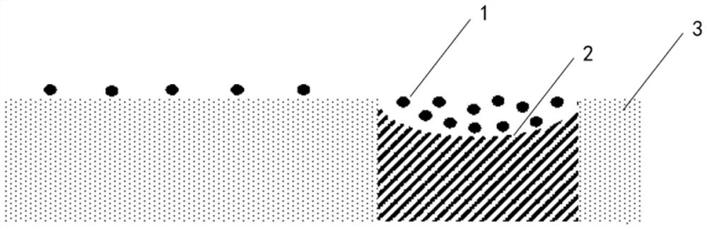
[0055] This embodiment provides a chemical mechanical polishing method for a wafer surface. For a schematic diagram of the wafer surface, see figure 1 , the chemical mechanical polishing method comprises the following steps:
[0056] (1) The first grinding with a pressure of 2.5 psi is performed on the surface of the wafer, and along with the injection of polishing liquid 1 with a flow rate of 290 mL / min to the surface of the wafer, the copper body on the groove of the wafer is removed to the surface of the obtained wafer. The thickness is 190nm;
[0057] (2) The surface of the wafer obtained in step (1) is subjected to a second grinding with a pressure of 1.8 psi, and along with injecting polishing liquid 1 with a flow rate of 290 mL / min to the surface of the wafer, the copper residues on the grooves of the wafer are removed. ;
[0058] (3) The pressure applied to the surface of the wafer obtained in step (2) is 0.9 psi, and the polishing rate is The over-polishing treatm...
Embodiment 2
[0063] This embodiment provides a chemical mechanical polishing method for a wafer surface. For a schematic diagram of the wafer surface, see figure 1 , the chemical mechanical polishing method comprises the following steps:
[0064] (1) The first grinding with a pressure of 2 psi is performed on the surface of the wafer, and along with the injection of polishing liquid 1 with a flow rate of 280 mL / min to the surface of the wafer, the copper body on the groove of the wafer is removed to the thickness of the obtained wafer is 200nm;
[0065] (2) The second grinding with a pressure of 1.5 psi is performed on the surface of the wafer obtained in step (1), and the polishing solution 1 with a flow rate of 280 mL / min is injected onto the surface of the wafer to remove the copper residue on the groove of the wafer. ;
[0066] (3) The pressure applied to the surface of the wafer obtained in step (2) is 0.8 psi, and the polishing rate is The over-polishing treatment, accompanied by...
Embodiment 3
[0071] This embodiment provides a chemical mechanical polishing method for a wafer surface. For a schematic diagram of the wafer surface, see figure 1 , the chemical mechanical polishing method comprises the following steps:
[0072] (1) The first grinding with a pressure of 3 psi is performed on the surface of the wafer, and along with the injection of polishing liquid 1 with a flow rate of 300 mL / min to the surface of the wafer, the copper body on the groove of the wafer is removed to the thickness of the obtained wafer. is 180nm;
[0073] (2) the second grinding that the applied pressure is 2psi is carried out to the wafer surface obtained in step (1), and along with the injection flow rate of 300mL / min of polishing liquid 1 to the wafer surface, the copper residue on the wafer groove is removed;
[0074] (3) The pressure applied to the surface of the wafer obtained in step (2) is 1 psi, and the polishing rate is The over-polishing treatment, accompanied by the injection...
PUM
| Property | Measurement | Unit |
|---|---|---|
| thickness | aaaaa | aaaaa |
| thickness | aaaaa | aaaaa |
Abstract
Description
Claims
Application Information