Manufacturing method of flexible amoled display

A manufacturing method and display technology, applied in semiconductor/solid-state device manufacturing, semiconductor devices, electric solid-state devices, etc., can solve the problems of flexible substrate 200 protrusions and depressions, cleaning, flexible substrate 200 damage, etc., to achieve the improvement of resistance Water and oxygen barrier performance, high degree of planarization, and the effect of ensuring optical performance

Active Publication Date: 2019-10-18
WUHAN CHINA STAR OPTOELECTRONICS TECH CO LTD
View PDF6 Cites 0 Cited by
  • Summary
  • Abstract
  • Description
  • Claims
  • Application Information

AI Technical Summary

Problems solved by technology

[0010] In the above method for manufacturing a flexible AMOLED display, since the initial Clean in the step 1' cannot completely clean the impurity particles (Particles) on the glass substrate 100, the surface of the glass substrate 100 is rough, so in such a The flexible substrate 200 formed on the glass substrate 100 is prone to poor protrusions and depressions; and, in the case of the rough surface of the glass substrate 100, the flexible substrate 200 is easily combined with the glass substrate 100 tightly, resulting in the The laser lift-off process in step 4' cannot completely peel off the flexible substrate 200 from the glass substrate 100, resulting in a fine polyimide film layer remaining on the glass substrate 100, so that the flexible substrate 200 The bottom 200 is damaged; the above two factors can cause the flattening degree of the flexible substrate 200 to decrease, reduce the water and oxygen barrier performance of the flexible substrate 200, and make the external water vapor and oxygen easily enter the flexible AMOLED. In the display 600, the thin film transistor array layer 300 above the flexible substrate 200 is corroded, and at the same time, the decrease in the planarization degree of the flexible substrate 200 will also affect the optical performance of the flexible AMOLED display 600

Method used


Image

  • Manufacturing method of flexible amoled display
  • Manufacturing method of flexible amoled display
  • Manufacturing method of flexible amoled display

Examples


Embodiment Construction

[0038] In order to further illustrate the technical means adopted by the present invention and its effects, the following describes in detail in conjunction with preferred embodiments of the present invention and accompanying drawings.

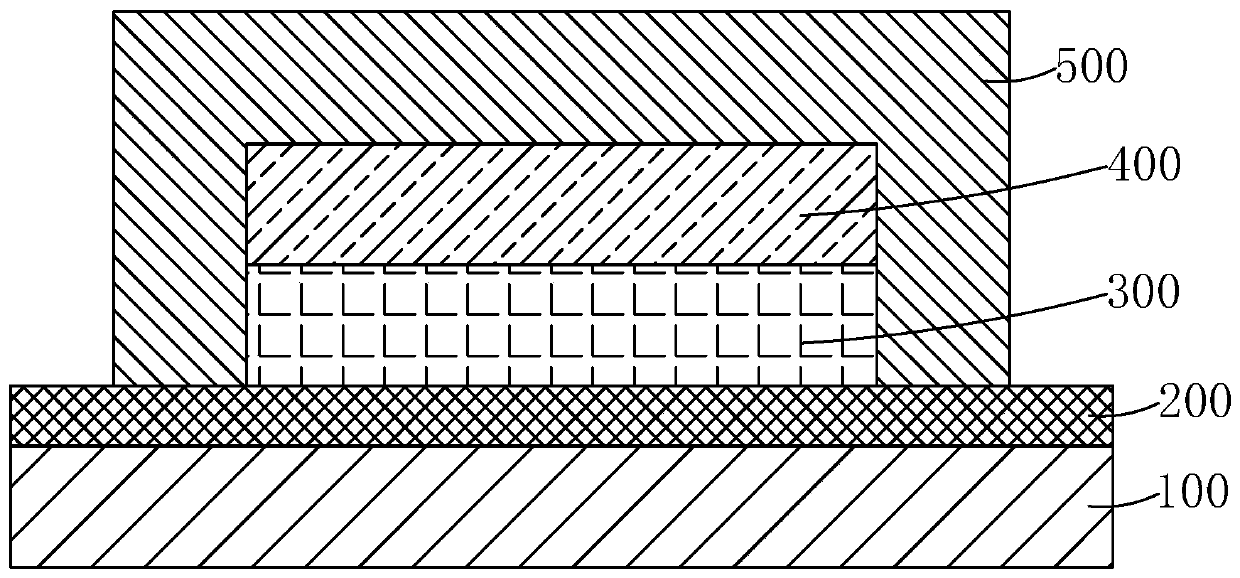
[0039] see Figure 5 , the invention provides a method for manufacturing a flexible AMOLED display, comprising the steps of:

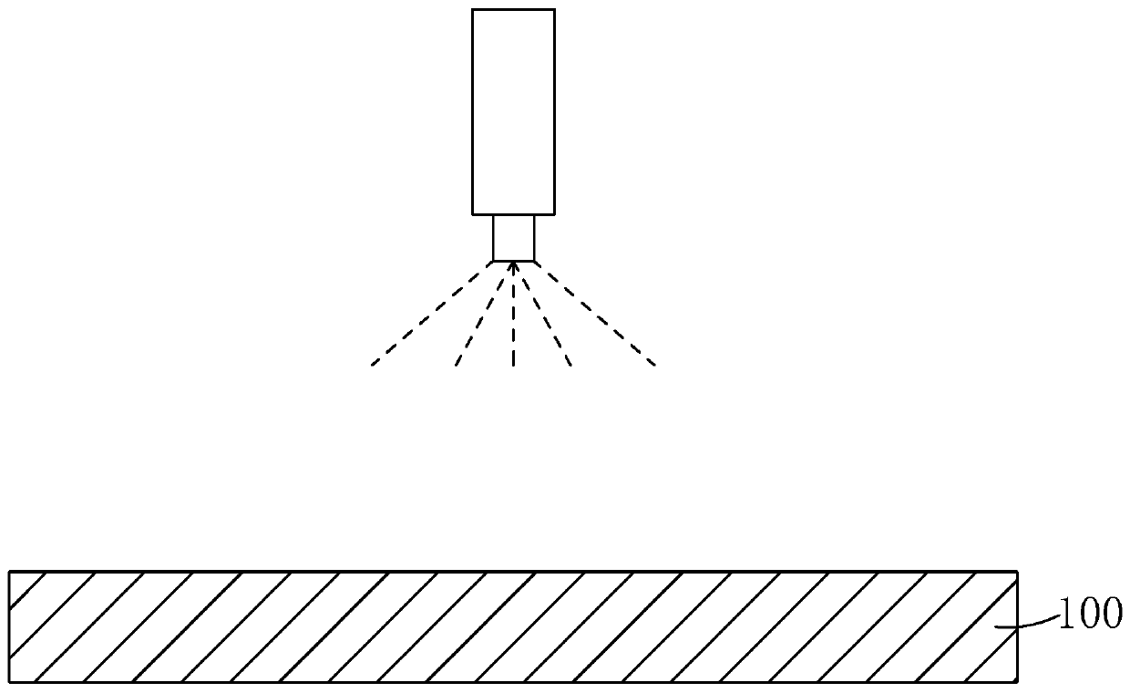
[0040] Step 1, such as Image 6 As shown, a rigid substrate 10 is provided, and the rigid substrate 10 is cleaned (initialClean).

[0041] Specifically, in the step 1, the rigid substrate 10 is a glass substrate.

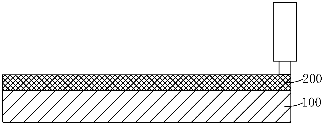
[0042] Step 2, such as Figure 7 As shown, an inorganic film layer 20 with a flat surface is formed on the rigid substrate 10 .

[0043] Specifically, in the step 2, the inorganic film layer 20 is formed by using plasma enhanced chemical vapor deposition (PECVD, PlasmaEnhanced Chemical Vapor Deposition).

[0044] The inorganic film layer 20 can improve the planarization degree of the surface of the rigid ...


PUM

PropertyMeasurementUnit
thicknessaaaaaaaaaa
thicknessaaaaaaaaaa

Abstract

The invention provides a method for manufacturing a flexible AMOLED display. Before making a flexible substrate on a rigid substrate, firstly, an inorganic film layer with a flat surface is formed on the rigid substrate, and then a polymeric film is coated on the inorganic film layer. material to form a flexible substrate, which can not only avoid the problem of sag and protrusion of the flexible substrate caused by impurity particles remaining on the surface of the rigid substrate due to poor cleaning, but also make the flexible substrate and the rigid substrate peel off. The substrate is easily separated from the rigid substrate to protect the flexible substrate from damage, so that the flexible substrate of the flexible AMOLED display has a higher degree of planarization, improves the water and oxygen barrier performance of the flexible substrate, and ensures flexibility. Optical properties of AMOLED displays.

Description

technical field [0001] The invention relates to the field of display technology, in particular to a method for manufacturing a flexible AMOLED display. Background technique [0002] Organic Light-Emitting Diode (OLED) display, also known as organic electroluminescent display, is an emerging flat panel display device, due to its simple preparation process, low cost, low power consumption, high luminance, Wide range of working temperature, light and thin size, fast response speed, easy to realize color display and large-screen display, easy to realize matching with integrated circuit driver, easy to realize flexible display, etc., so it has broad application prospects. [0003] According to the driving method, OLED can be divided into two categories: passive matrix OLED (Passive Matrix OLED, PMOLED) and active matrix OLED (Active Matrix OLED, AMOLED), namely direct addressing and thin film transistor (TFT, Thin Film Transistor) There are two types of matrix addressing. Among...

Claims


Application Information

Patent Timeline
Patent Type & Authority Patents(China)
IPC IPC(8): H01L27/32H01L51/56H01L51/52
CPCH10K59/12H10K50/80H10K59/1201H10K71/00
Inventor 李朝邱立峯
Owner WUHAN CHINA STAR OPTOELECTRONICS TECH CO LTD
Why Eureka
Try Eureka