Polishing layer, polishing pad and preparation method

A polishing layer and polishing pad technology, which is applied in grinding/polishing equipment, manufacturing tools, metal processing equipment, etc. Effect of meta wear rate

Active Publication Date: 2020-12-08
HUBEI DINGHUI MICROELECTRONICS MATERIALS CO LTD +1
View PDF9 Cites 0 Cited by
  • Summary
  • Abstract
  • Description
  • Claims
  • Application Information

AI Technical Summary

Problems solved by technology

Secondly, the degree of adhesion between the polishing pad and the wafer will decrease with the increase of the warping degree of the polishing layer. The uneven polishing surface will lead to inconsistent removal degrees in different areas of the wafer during the grinding process, thus reducing the surface of the wafer. Flatness

Method used


Image

  • Polishing layer, polishing pad and preparation method
  • Polishing layer, polishing pad and preparation method
  • Polishing layer, polishing pad and preparation method

Examples


Embodiment 1

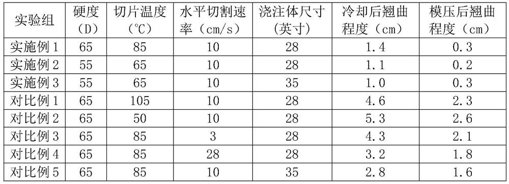
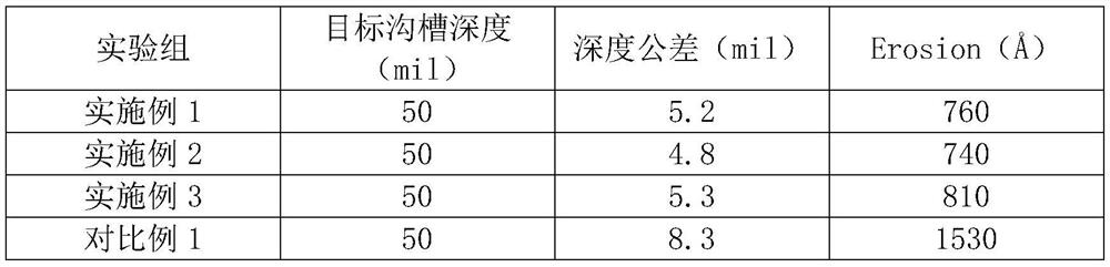
[0089] Casting body a (65D, 28 inches) is cooled to 90°C within 2 hours and taken out. Move the mold to a slicer to fix it, and adjust the horizontal moving speed of the slicer knife to 10cm / min. The cast body was heated with an infrared lamp and kept at 90°C. Start slicing after 10 min of incubation. The sliced ​​sample was placed flat and cooled at 25°C for 12 hours. The Shore hardness was tested to be 65D. The die was pressed flat for 12 hours to measure the warpage of the die before and after molding (the five points with the largest warpage and the distance between the five points on the horizontal plane) mean height difference), the results are shown in Table 1.

Embodiment 2

[0091] The pouring body b (55D, 28 inches) was cooled to 65°C within 2 hours and then taken out. Move the mold to a slicer to fix it, and adjust the horizontal moving speed of the slicer knife to 10cm / min. The cast body was heated with an infrared lamp and kept warm to 65°C. Start slicing after 10 min of incubation. The sliced ​​samples were placed flat and cooled at 25°C for 12 hours. The Shore hardness was tested to be 55D. The dies were pressed flat for 12 hours to measure the warpage of the die before and after molding. The results are shown in Table 1.

Embodiment 3

[0093] The casting body b (55D, 35 inches) was cooled to 65°C within 2 hours and then taken out. Move the mold to a slicer to fix it, and adjust the horizontal moving speed of the slicer knife to 10cm / min. The cast body was heated with an infrared lamp and kept warm to 65°C. Start slicing after 10 min of incubation. The sliced ​​samples were placed flat and cooled at 25°C for 12 hours. The Shore hardness was tested to be 55D. The dies were pressed flat for 12 hours to measure the warpage of the die before and after molding. The results are shown in Table 1.


PUM

PropertyMeasurementUnit
Shore hardnessaaaaaaaaaa
densityaaaaaaaaaa
thicknessaaaaaaaaaa

Abstract

The invention provides a polishing layer, a polishing pad with the polishing layer and a preparation method of the polishing layer, and relates to the technical field of polishing of chemical mechanical planarization treatment. The preparation method comprises the following steps that prepolymer of bifunctional or polyfunctional isocyanate in component A and a multi-component mixture of a hollow microsphere in component B and a curing agent in component C are prepared; forming by pouring is carried out, specifically, the multi-component mixture is poured into a mould cavity and subjected to leveling gelation; heating and solidifying are carried out, specifically, a mould loading a gelatinous ternary mixture is heated and solidified, to obtain a pouring body; and when the temperature is lowered to a predetermined temperature T, the heat preservation and slice cutting are performed, and the horizontal cutting rate V of a cutter relative to the pouring body during slice cutting meets: 8cm / s <= V<= 20 cm / s.

Description

technical field [0001] The invention relates to the technical field of chemical mechanical planarization polishing, in particular to a polishing layer for a chemical mechanical polishing pad, a polishing pad and a preparation method. Background technique [0002] In the manufacture of integrated circuits and other electronic devices, it is necessary to remove the layers of conductive materials, semiconductor materials and dielectric materials deposited on the surface of semiconductor wafers or (wafers, Wafer). Chemical Mechanical Polishing or Chemical Mechanical Polishing (CMP) is currently the most commonly used technique for surface polishing of workpieces. CMP is a technology that combines chemical erosion and mechanical removal, and is also the most commonly used technology for planarization (planarization) such as semiconductor wafers. [0003] At present, in the conventional CMP process, the polishing pad for polishing is installed on the support assembly of the equip...

Claims


Application Information

Patent Timeline
Patent Type & Authority Patents(China)
IPC IPC(8): B24B37/20B24B37/22B24B37/24B24D18/00C08G18/66C08G18/48C08G18/32C08G18/10C08J9/32C08L75/08
CPCB24B37/20B24B37/22B24B37/24B24D18/0009C08G18/10C08G18/3814C08G18/4854C08G18/6685C08J9/32C08J2203/22C08J2375/08
Inventor 李翔刘敏童已仁吴晓茜朱顺全
Owner HUBEI DINGHUI MICROELECTRONICS MATERIALS CO LTD
Why Eureka
Try Eureka