A way to add redundant graphics

A technology of redundant graphics and graphics, applied in the direction of electrical components, semiconductor/solid-state device manufacturing, circuits, etc., can solve the problem that the density of sub-regions with the same density varies greatly.

Active Publication Date: 2016-09-07
SHANGHAI HUALI MICROELECTRONICS CORP
View PDF5 Cites 0 Cited by
  • Summary
  • Abstract
  • Description
  • Claims
  • Application Information

AI Technical Summary

Problems solved by technology

However, there is no distinction between the redundant graphics added to each sub-area under the same density area, so that some redundant graphics of a specific size can only be added to some sub-areas, while the remaining sub-areas of the same density range are not added. , which will lead to a large difference in the density of several sub-regions with the same density after adding redundant graphics

Method used


Image

  • A way to add redundant graphics
  • A way to add redundant graphics
  • A way to add redundant graphics

Examples


Embodiment Construction

[0029] Embodiments embodying the features and advantages of the present invention will be described in detail in the following description. It should be understood that the invention can have various changes in different examples without departing from the scope of the invention, and that the descriptions and illustrations therein are illustrative in nature rather than limiting the invention.

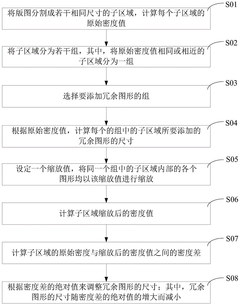
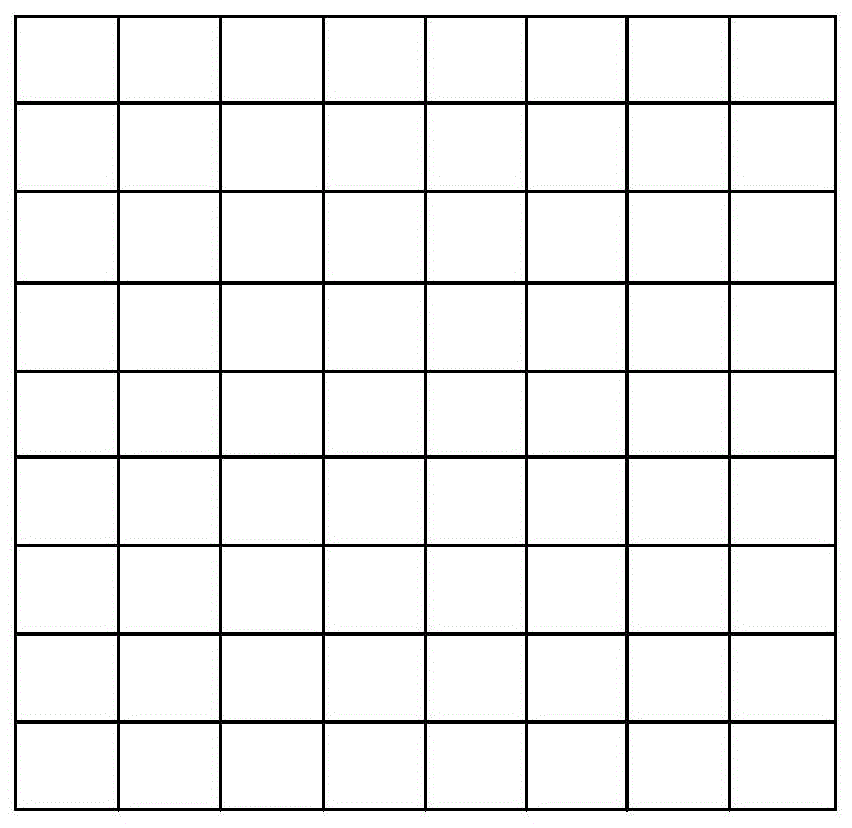
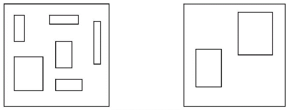
[0030] The following is attached Figure 1-4 , the method for adding redundant graphics of the present invention will be further described in detail through specific embodiments. figure 1 It is a schematic flowchart of a method for adding redundant graphics in a preferred embodiment of the present invention, figure 2 It is a schematic diagram of the divided layout used in the method for adding redundant graphics in the above-mentioned preferred embodiment of the present invention, image 3 is a schematic diagram of any two sub-regions in the layout in the above-mentioned preferred em...


PUM


Abstract

The invention provides a method for adding redundant graphics. The method comprises the following steps: dividing a domain into a plurality of subdomains in the same size and calculating an original density value of each subdomain; dividing the subdomains into a plurality of groups and taking the subdomains with the same or similar original density values as one group; selecting the groups in which the redundant graphics need to be added; calculating the sizes of the redundant graphics needing to be added in the subdomains of each group according to the density values; setting a scaling value and scaling each of the redundant graphics in the subdomains of the same group according to the scaling value; calculating the scaled density values of the subdomains; calculating a density difference of the original density values and the scaled density values of the subdomains; and adjusting the sizes of the redundant graphics according to an absolute value of the density difference, wherein the sizes of the redundant graphics are decreased along with the increasing of the absolute value of the density difference. According to the method, the homogeneous density distribution of wafers is ensured; the density distribution difference of the domain and the wafers is reduced, so that the flatness degree is improved.

Description

technical field [0001] The invention relates to the technical field of semiconductor manufacturing, in particular to a method for adding redundant graphics. Background technique [0002] As chip manufacturing technology nodes become smaller and process technology becomes more and more complex, the degree of wafer planarization after chemical mechanical polishing (CMP, Chemical Mechanical Polishing) has an increasing impact on devices or structures. [0003] However, for metal planarization, the metal and dielectric materials typically have different removal rates, and the selectivity of these materials for the removal rate can lead to unwanted erosion and dishing of the wafer. Erosion will occur if the dielectric is too thin locally, and the grinding rate of the metal is higher than that of the dielectric, and depressions will appear near the contact surface of the two. The chemical mechanical polishing process in the existing production process also encounters the same pro...

Claims


Application Information

Patent Timeline
Patent Type & Authority Patents(China)
IPC IPC(8): H01L21/60
Inventor 倪晟于世瑞毛智彪张瑜
Owner SHANGHAI HUALI MICROELECTRONICS CORP
Why Eureka
Try Eureka