Power semiconductor device

A technology of power semiconductors and positive conductors, which is applied in the direction of semiconductor devices, output power conversion devices, semiconductor/solid-state device components, etc., can solve the problems of low design freedom, capacitor size and capacitor quantity limitation, and achieve miniaturization of wiring inductance , The effect of reducing wiring inductance

Pending Publication Date: 2021-09-03
HITACHI LTD
View PDF1 Cites 0 Cited by
  • Summary
  • Abstract
  • Description
  • Claims
  • Application Information

AI Technical Summary

Problems solved by technology

[0003] In the power semiconductor device described in Patent Document 1, since the power semiconductor element part and the capacitor are arranged on the same surface of the negative electrode conductor part and the positive electrode conductor part, it is necessary to adjust the thickness of the capacitor to the thickness of the power semiconductor element part. Low degrees of freedom, limited capacitor size and number of capacitors available per power semiconductor device

Method used


Image

  • Power semiconductor device
  • Power semiconductor device
  • Power semiconductor device

Examples


Embodiment Construction

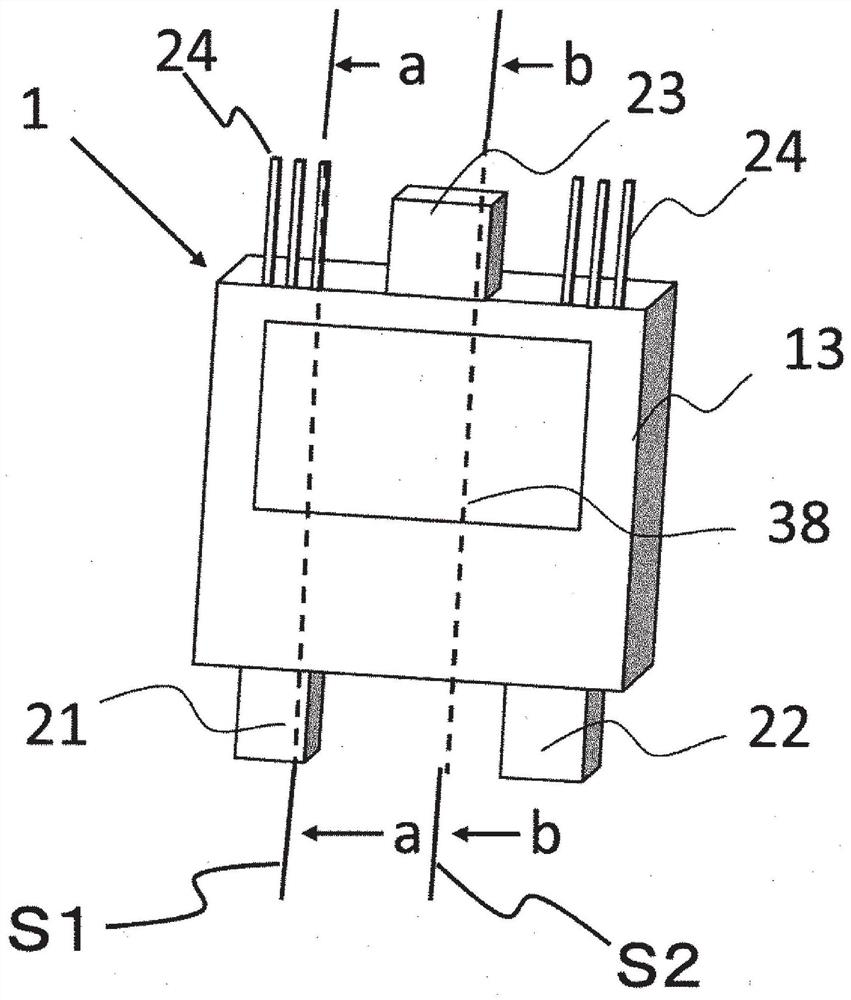
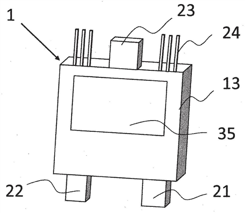
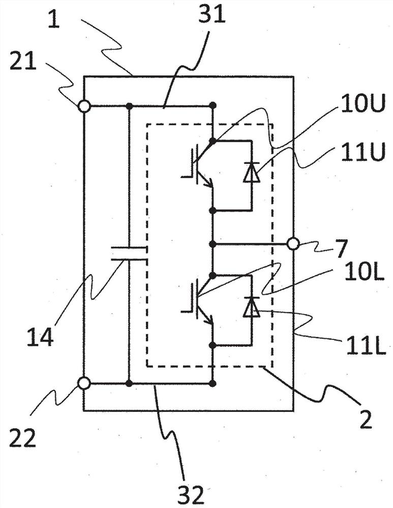
[0027] Hereinafter, as an embodiment of the structured body of the present invention, a power semiconductor device used for a power conversion device mounted on a vehicle will be described. A power semiconductor element, a conductor portion on which the power semiconductor element is mounted, and a ceramic substrate as an insulating resin plate electrically connected to the conductor plate will be described with reference to the drawings. In addition, the same reference numerals are assigned to the same elements in each figure, and overlapping explanations are omitted.

[0028] FIG. 1( a ) is an overall perspective view viewed from one side of the power semiconductor device 1 of the present embodiment. FIG. 1( b ) is an overall perspective view of the power semiconductor device 1 according to the present embodiment seen from the other side. Figure 4 It is a cross-sectional view of the power semiconductor device 1 viewed from the arrow direction a on the plane S1 of FIG. 1( a...


PUM


Abstract

The present invention addresses the problem of achieving low inductance of wiring in a power semiconductor device provided with smoothing capacitors and size reduction of the power semiconductor device. A power semiconductor device according to the present invention is provided with: a power semiconductor circuit section; a plurality of smoothing capacitors; a positive electrode conductor section and a negative electrode conductor section; and a sealing material. The plurality of smoothing capacitors constitute a capacitor circuit section sandwiched between the positive electrode conductor section and the negative electrode conductor section. The power semiconductor circuit section has: a first exposed surface that is exposed from the sealing material; and a second exposed surface that is exposed from the sealing material and that is provided on the opposite side from said first exposed surface. When a plane overlapping the first exposed surface is defined as a first plane and a plane overlapping the second exposed surface is defined as a second plane, the capacitor circuit section is formed so as to be placed in a space between the first plane and the second plane. The positive electrode conductor section or the negative electrode conductor section forms a recessed section for accommodating some of the plurality of smoothing capacitors.

Description

technical field [0001] The present invention relates to a power semiconductor device, and more particularly to a power semiconductor device used in a power conversion device for converting DC power into AC power. Background technique [0002] Against the background of increasing environmental restrictions, the market for inverters for EVs is growing rapidly worldwide. On the other hand, inverters driven by high carrier frequency such as SiC are attracting attention, and a low inductance structure for realizing high carrier frequency drive is required. [0003] In the power semiconductor device described in Patent Document 1, since the power semiconductor element part and the capacitor are arranged on the same surface of the negative electrode conductor part and the positive electrode conductor part, it is necessary to adjust the thickness of the capacitor to the thickness of the power semiconductor element part. The degree of freedom is low, and the size of the capacitors a...

Claims


Application Information

Patent Timeline
IPC IPC(8): H01L25/07H01L25/18H02M7/48
CPCH01L25/18H02M7/003H02M7/5387H01L2224/32245H01L2224/40137H01L2224/33181H01L2924/19041H01L2924/19105H01L2224/73221H01L2224/73263H01L2224/73265H01L2224/48227H01L23/49589H01L23/3735H01L23/49562H01L23/49575H01L23/49531H01L23/4334H01L23/5385H01L25/072H01L25/16H01L2924/13055H01L2224/45124H01L24/45H01L2224/48091H01L2224/29101H01L2224/83801H01L2224/8384H01L24/29H01L24/83H01L24/40H01L24/48H01L2924/181H01L2224/49113H01L24/32H01L24/06H01L2224/04026H01L2224/04034H01L2224/04042H01L24/73H01L24/84H01L2224/84801H01L2224/8484H01L2924/1203H01L2224/40195H01L2224/40245H01L2924/00H01L2924/00014H01L2924/014H01L2924/00012
Inventor 望月诚仁井出英一长崎仁德田中信太朗平尾高志楠川顺平露野円丈
Owner HITACHI LTD
Why Eureka
Try Eureka