Power semiconductor device module

a technology of semiconductor devices and semiconductor devices, applied in semiconductor devices, semiconductor/solid-state device details, instruments, etc., can solve the problems of difficulty in miniaturization, the limitation of miniaturization of principal current wiring, and the increase of the number of external terminals of the power semiconductor device module, so as to reduce reduce the wiring inductance. , the effect of reducing the number of external terminals

Inactive Publication Date: 2015-08-25
MITSUBISHI ELECTRIC CORP
View PDF17 Cites 1 Cited by
  • Summary
  • Abstract
  • Description
  • Claims
  • Application Information

AI Technical Summary

Benefits of technology

[0010]An object of the present invention is to miniaturize a power semiconductor device module by reducing the number of external terminals as much as possible, and to reduce wiring inductance.
[0012]According to the power semiconductor device module, since the number of control terminals for temperature detection can be reduced, the power semiconductor device module can be miniaturized.

Problems solved by technology

Hence, the number of external terminals of the power semiconductor device module has significantly increased, and miniaturization of principal current wiring has reached a limit.
Hence, the power semiconductor device module described in Japanese Patent Application Laid-Open No. 2011-249364 has difficulty in miniaturization due to a large number of control terminals.
In addition, there is a problem that wiring inductance is large, since wiring on the direct-current high-voltage side and wiring on the direct-current low-voltage side are provided at distant locations.

Method used


Image

  • Power semiconductor device module
  • Power semiconductor device module
  • Power semiconductor device module

Examples


first preferred embodiment

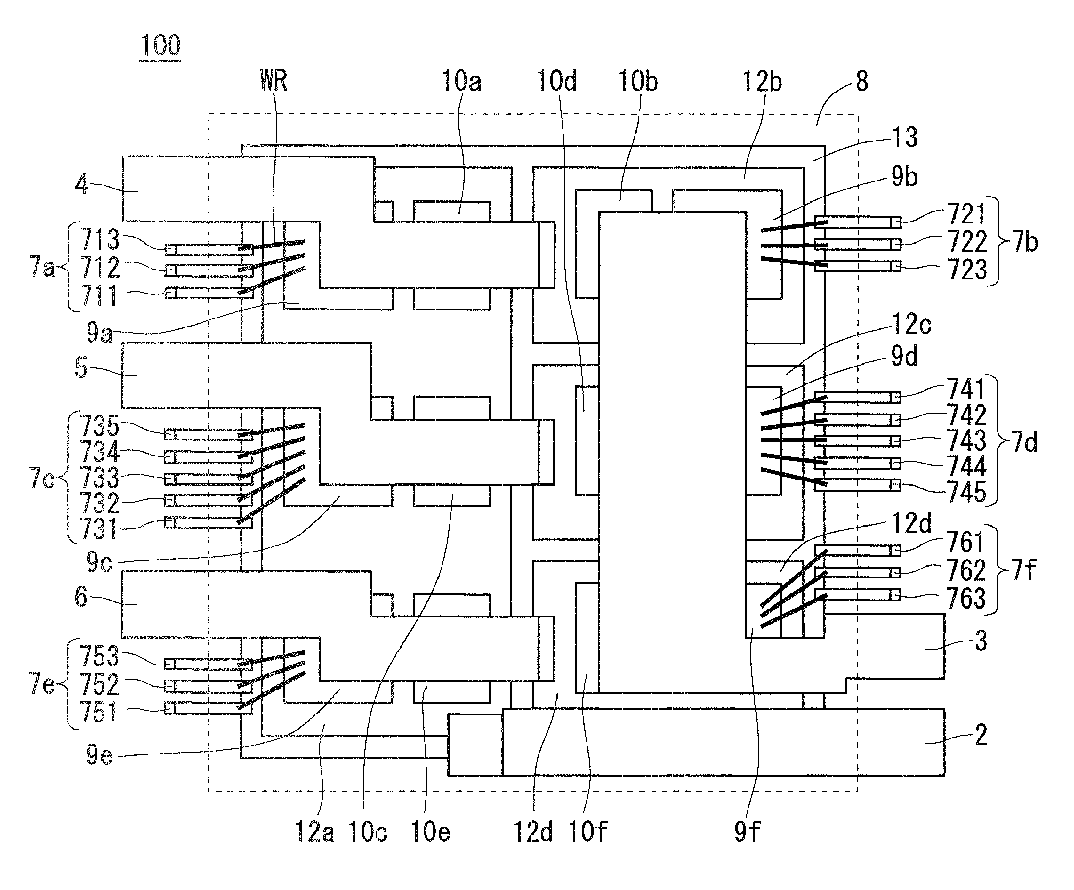
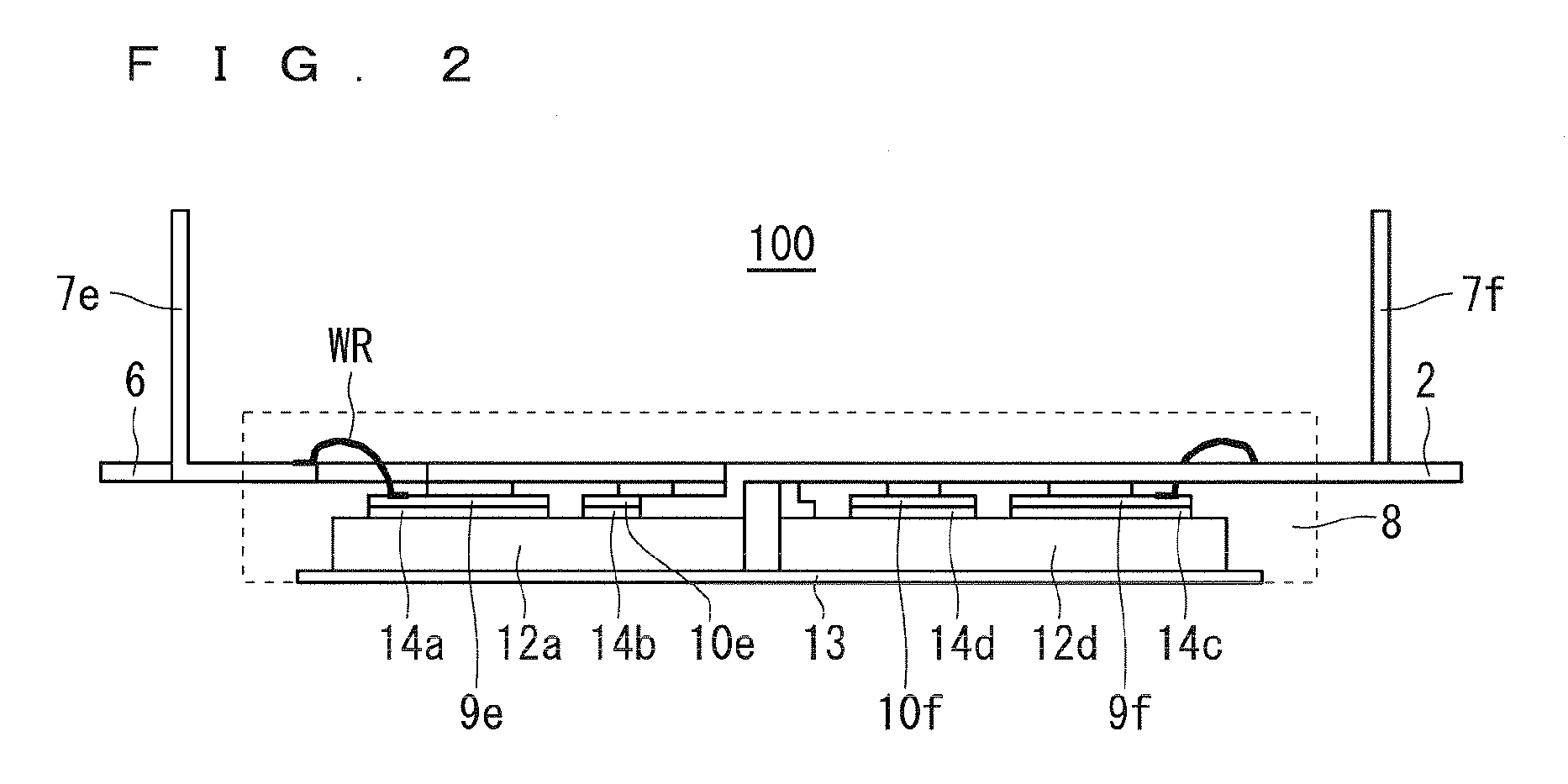
[0024]FIG. 1 is a plan view showing a configuration of a power semiconductor device module 100 of a first preferred embodiment according to the present invention, and FIG. 2 is a side view as viewed from the side of a direct-current high-voltage terminal 2. In both drawings, a mold resin 8 is omitted. FIG. 3 is a circuit diagram showing a configuration of the power semiconductor device module 100.

[0025]As shown in FIG. 3, the power semiconductor device module 100 includes six semiconductor chip groups 11a, 11b, 11c, 11d, 11e, and 11f including IGBT chips 9a, 9b, 9c, 9d, 9e, and 9f having a temperature detection function; and diode chips 10a, 10b, 10c, 10d, 10e, and 10f which are connected in anti-parallel with the IGBT chips 9a to 9f, respectively.

[0026]The semiconductor chip groups 11a and 11b in a set, the semiconductor chip groups 11c and 11d in a set, and the semiconductor chip groups 11e and 11f in a set each are connected in series with each other, and output terminals 4, 5, a...

second preferred embodiment

[0064]FIG. 4 is a plan view showing a configuration of a power semiconductor device module 200 of a second preferred embodiment according to the present invention, and FIG. 5 is a side view as viewed from the side of a direct-current high-voltage terminal 21. In both drawings, a mold resin 25 is omitted. FIG. 6 is a circuit diagram showing a configuration of the power semiconductor device module 200.

[0065]As shown in FIG. 6, the power semiconductor device module 200 includes four semiconductor chip groups 28a, 28b, 28c, and 28d including IGBT chips 26a, 26b, 26c, and 26d having a temperature detection function; and diode chips 27a, 27b, 27c, and 27d which are connected in anti-parallel with the IGBT chips 26a to 26d, respectively.

[0066]The semiconductor chip groups 28a and 28b in a set and the semiconductor chip groups 28c and 28d in a set each are connected in parallel with each other, and the set of the semiconductor chip groups 28a and 28b and the set of the semiconductor chip gr...

third preferred embodiment

[0094]FIG. 7 is a plan view showing a configuration of a power semiconductor device module 300 of a third preferred embodiment according to the present invention, and FIG. 8 is a side view as viewed from the side of a direct-current high-voltage terminal 31 and a direct-current low-voltage terminal 32. In both drawings, a mold resin 8 is omitted.

[0095]Note that the power semiconductor device module 300 has the same circuit configuration as the power semiconductor device module 100 of the first preferred embodiment, and is configured as a three-phase inverter circuit and includes control terminals for detecting currents and temperatures to protect IGBT chips from overcurrent and overheat. Note that the same components as those of the power semiconductor device module 100 shown in FIGS. 1 and 2 are denoted by the same reference characters and overlapping description is omitted.

[0096]As shown in FIG. 7, in the power semiconductor device module 300, the direct-current high-voltage termi...


PUM


Abstract

A power semiconductor device module includes a plurality of inverters, each having a first transistor and a second transistor that are interposed in series between a first potential and a second potential and that operate complementarily. The plurality of inverters are assembled into a module. Only one predetermined inverter of the plurality of inverters is configured to detect temperatures of the first and second transistors, and control terminals for detection of the temperatures of the first and second transistors protrude from sides of the module.

Description

BACKGROUND OF THE INVENTION[0001]1. Field of the Invention[0002]The present invention relates to a power semiconductor device module having mounted thereon a voltage drive type semiconductor device such as IGBT (Insulated Gate Bipolar Transistor).[0003]2. Description of the Background Art[0004]In a power semiconductor device module, an electrical wiring connected to a semiconductor device mounted on the module is generally made from copper or the like which has a low electrical resistance and is inexpensive. The current density is designed such that heat generation upon passage of current does not exceed the heat-resistant temperature of the semiconductor device and the members composing the power semiconductor device module.[0005]Meanwhile, miniaturization of the power semiconductor device module has been advanced year by year due to a reduction in the loss of semiconductor device mounted on the module and improvements in cooling performance and insulation performance. Along with t...

Claims


Application Information

Patent Timeline
Patent Type & Authority Patents(United States)
IPC IPC(8): H01L25/00H01L23/00G05F1/10
CPCG05F1/10H01L24/34H01L2224/48091H01L2224/48247H01L2224/48472H01L2924/1305H01L2924/13055H01L2924/00014H01L2924/00H01L2224/40137H01L2924/181H01L24/36H01L24/40H01L2224/73221H01L2224/83801H01L24/83H01L2224/0603H01L2924/00012H01L2224/37099H01L2224/84
Inventor USUI, OSAMU
Owner MITSUBISHI ELECTRIC CORP
Why Eureka
Try Eureka