Semiconductor structure and forming method thereof

A semiconductor and intermediate structure technology, applied in semiconductor devices, semiconductor/solid-state device manufacturing, electrical components, etc., can solve problems such as device performance needs to be improved

Active Publication Date: 2021-09-14
SEMICON MFG INT TIANJIN +1
View PDF10 Cites 0 Cited by
  • Summary
  • Abstract
  • Description
  • Claims
  • Application Information

AI Technical Summary

Problems solved by technology

[0004] However, the performance of devices for...

Method used


Image

  • Semiconductor structure and forming method thereof
  • Semiconductor structure and forming method thereof
  • Semiconductor structure and forming method thereof

Examples


Embodiment Construction

[0017] It can be seen from the background art that the performance of devices formed by existing processes still needs to be improved. The reason why the performance of the device needs to be improved is analyzed in combination with a method of forming a semiconductor structure.

[0018] Specifically, after the small-scale structures are formed, these small-scale structures are usually further processed. However, due to the small size of these small-scale structures, it is too difficult to control their processing, which can easily cause these small-scale structures. The morphology of the dimensional structure is poor, which in turn affects the performance of the device.

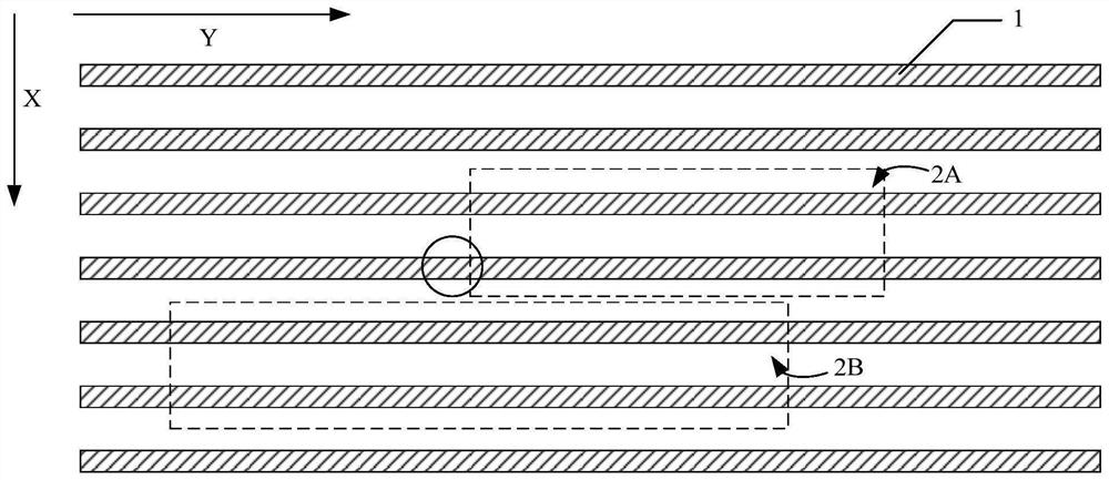
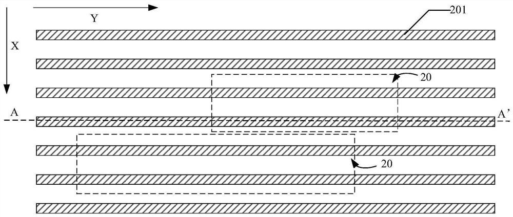
[0019] For example, refer to figure 1 , in the process of forming a semiconductor device, it is necessary to remove the fins outside the device area (such as etching), whether it is directly processing the fins in the graphics area to be treated, or the fins used to form the fins in the graphics area to be ...


PUM


Abstract

The invention discloses a semiconductor structure and a forming method thereof. The method comprises the following steps: providing a substrate, and forming a to-be-processed structure on the substrate, wherein the substrate comprises a to-be-processed graphic region, the to-be-processed graphic region comprises a part of the to-be-processed structure, and the length direction of the to-be-processed graphic region is the extension direction of the to-be-processed structure; removing to-be-processed structures at two ends of the to-be-processed graphic region, and taking the residual to-be-processed structures in the to-be-processed graphic region as intermediate structures; and removing the intermediate structure, and taking the residual to-be-processed structure on the substrate as the target structure, thereby realizing accurate control of the processing process of the to-be-processed structure, and improving the performance of the device.

Description

technical field [0001] The invention relates to the field of semiconductor manufacturing, in particular to a semiconductor structure and a forming method thereof. Background technique [0002] With the continuous development of ultra-large integrated circuits, the critical dimension (CD) of semiconductor devices is continuously reduced, and its manufacturing process is also facing many restrictions and challenges. In the case of smaller and smaller critical dimensions, how to improve the performance of small-scale graphics The accuracy and stability of the system has become a research hotspot in the industry. [0003] Self-aligned double patterning (SADP) method and self-aligned quadruple patterning (SAQP) method are patterning methods that have been favored in recent years. The density of the pattern formed on the substrate by the self-aligned double patterning method is twice the density of the pattern formed on the substrate by the photolithography process, so that 1 / 2 t...

Claims


Application Information

Patent Timeline
IPC IPC(8): H01L21/308H01L29/10
CPCH01L21/3086H01L21/3088H01L29/1033
Inventor 纪世良刘盼盼张海洋
Owner SEMICON MFG INT TIANJIN
Why Eureka
Try Eureka