
Electric structure and making method

A technology of electrical connection and part, which is applied in the field of electrical structure and its production, can solve the problems of increasing cost, achieve the effect of protecting integrity, cheap method, and prolonging fatigue life

Inactive Publication Date: 2004-01-07
IBM CORP
View PDF1 Cites 0 Cited by
  • Summary
  • Abstract
  • Description
  • Claims
  • Application Information

AI Technical Summary

Problems solved by technology

Although this method greatly extends the fatigue life of the BGA, it also increases the cost of the product due to the cost of the conductive plate and the process steps and related equipment required to manufacture the encapsulation structure

Method used


Image

  • Electric structure and making method
  • Electric structure and making method
  • Electric structure and making method

Examples


Embodiment Construction

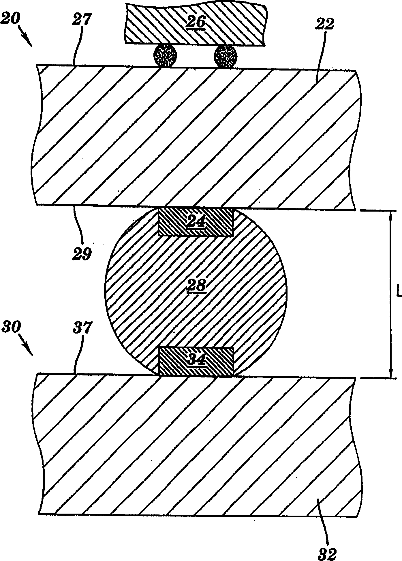
[0025] figure 1 A front cutaway view of BGA module 20 secured to circuit card 30 is shown. BGA module 20 includes dielectric substrate 22 , chip 26 secured to upper surface 27 of substrate 22 , BGA pads 24 secured to lower surface 29 of substrate 22 , and solder balls 28 of height L secured to BGA pads 24 . Circuit card 30 includes a dielectric board 32 and circuit card pads 34 secured to an upper surface 37 of board 32 . The circuit card can be any pre-wired board that includes dielectric material, such as the motherboard of a computer. Solder balls 28 are secured to pads 34 on circuit card 30 , thereby connecting BGA module 20 to circuit card 30 . Thermal strain on solder ball 28 generated during thermal cycling is distributed over height L. FIG. It is the intent of the present invention to modify the substrate 22 and / or plate 32, thereby redistributing the strain over heights greater than L to increase figure 1 fatigue life of the structure.

[0026] figure 2 shows a...


PUM


Abstract

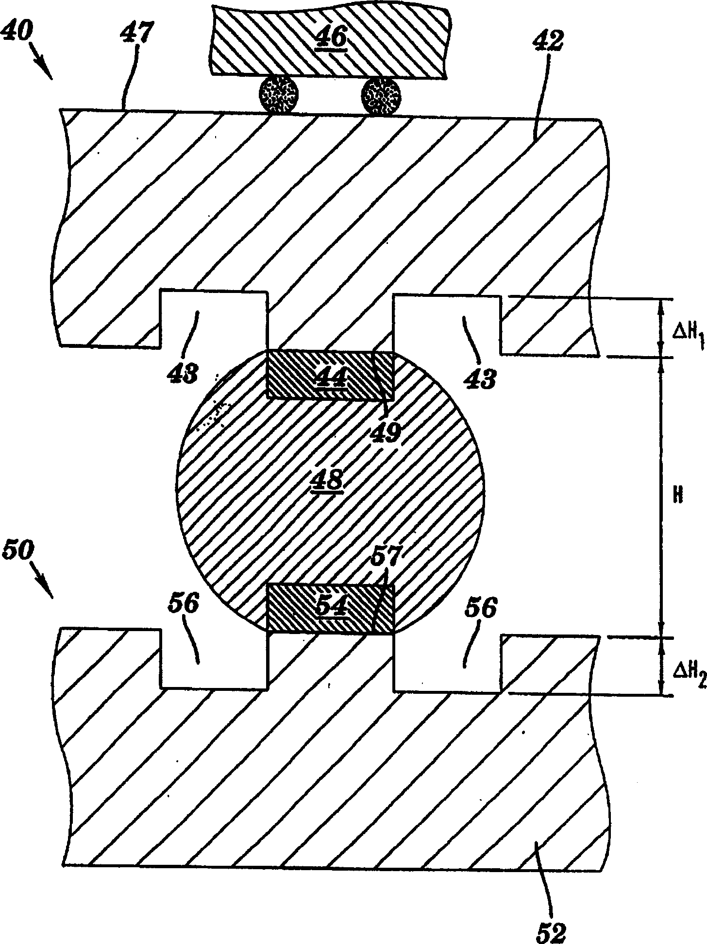
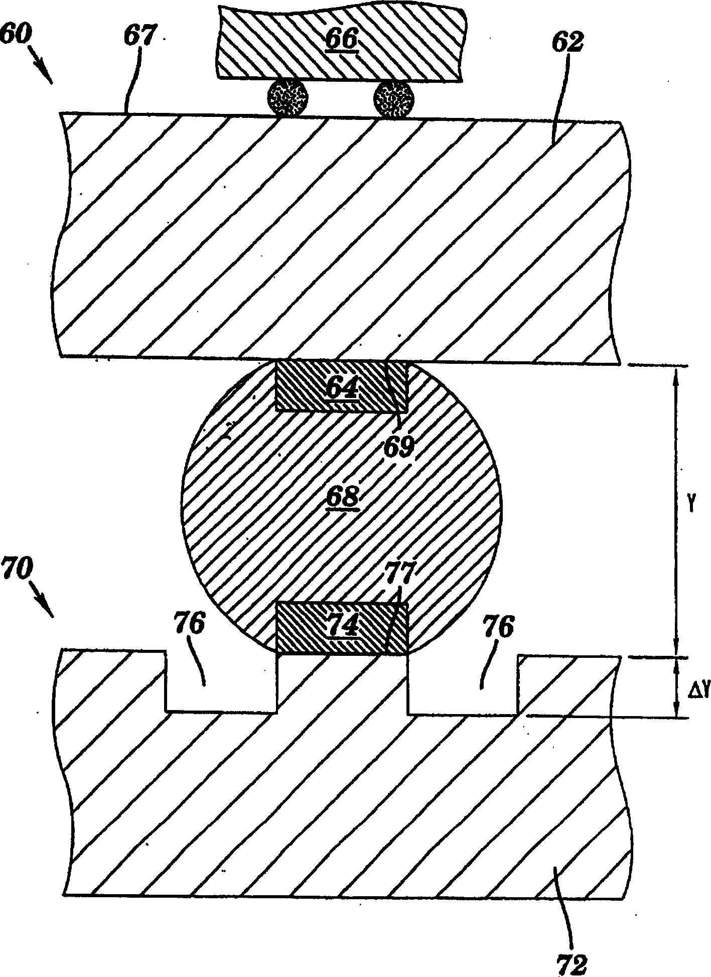
A method and structure for reducing thermally induced strains on the solder joints that couple a ball grid array (BGA) module to a circuit card, so as to improve the fatigue life of the BGA module. The thermally induced strains arise from a mismatch in thermal expansion coefficient between the dielectric substrate of the BGA module and the dielectric board of the circuit card. The method generates void annular regions around portions of the BGA dielectric substrate to which the BGA solder balls are to be attached and / or around portions of the circuit card dielectric material to which the BGA module is to be attached. This results in the formation of dielectric islands or peninsulas that bound the solder balls of the BGA module after installation on the circuit card. The dielectric islands or peninsulas thus formed serve to increase the effective height over which the differential expansion is accommodated, thereby reducing the strains throughout the solder joints. Additionally, the void annular regions provide space for the deformation of the dielectric islands or peninsulas, thereby increasing their compliance and transferring strain from the solder joints to the dielectric islands or peninsulas.

Description

technical field [0001] The present invention relates to structures and associated fabrication methods for reducing thermal strain in solder joints associated with connecting ball grid array (BGA) modules to solder balls of a circuit card. Background technique [0002] Modern board construction has a BGA module mounted on a circuit card. A BGA module includes a substrate having an upper surface and a lower surface of a dielectric material such as ceramic or plastic. An array of solder balls is secured to a corresponding array of conductive pads on the lower surface of the BGA module, while one or more chips are secured to the upper surface of the BGA module. A corresponding circuit card is a pre-wired board including a dielectric material and an array of conductive pads on the board. An example of a circuit card is the motherboard of a computer. The circuit card pads serve as anchor points for receiving one or more BGA modules. Thus, each solder ball on a BGA module mount...

Claims


Application Information

Patent Timeline
IPC IPC(8): H01L23/28H01L23/12H01L23/32H01L23/498H05K1/02H05K1/11H05K1/18H05K3/00H05K3/34
CPCH05K2201/09481H01L23/49816H01L2924/01025H05K2201/10734H01L2224/16H01L23/49838H01L2924/15311H05K3/0032H01L2924/0102H05K1/0271H01L2924/10253H05K2201/09036H01L2924/01087H05K3/3436H05K1/111Y10T29/49144Y10T29/49155Y02P70/50H01L2924/00H01L23/28
Inventor E·A·约翰逊J·S·克雷斯吉
Owner IBM CORP
Learn More