Aging circuit board, aging test structure and aging test method

A technology of aging test and aging circuit, which is applied in the direction of electronic circuit testing, printed circuit components, printed circuits connected with non-printed electrical components, etc., and can solve the problems of aging characteristics testing of small chip interconnection functions, etc.

Active Publication Date: 2021-09-24
HYGON INFORMATION TECH CO LTD
View PDF8 Cites 0 Cited by
  • Summary
  • Abstract
  • Description
  • Claims
  • Application Information

AI Technical Summary

Problems solved by technology

[0004] The purpose of the embodiment of the present application is to provide a burn-in circuit board, a burn-in test structure and a burn-in test method to improve the problem in the prior art that the aging characteristics of the interconnection function between small chips cannot be tested

Method used


Image

  • Aging circuit board, aging test structure and aging test method
  • Aging circuit board, aging test structure and aging test method
  • Aging circuit board, aging test structure and aging test method

Examples


Embodiment Construction

[0029] In order to make the purpose, technical solution and advantages of the present application clearer, the present application will be further described in detail below in conjunction with the accompanying drawings and embodiments. It should be understood that the specific embodiments described here are only used to explain the present application, and are not intended to limit the present application.

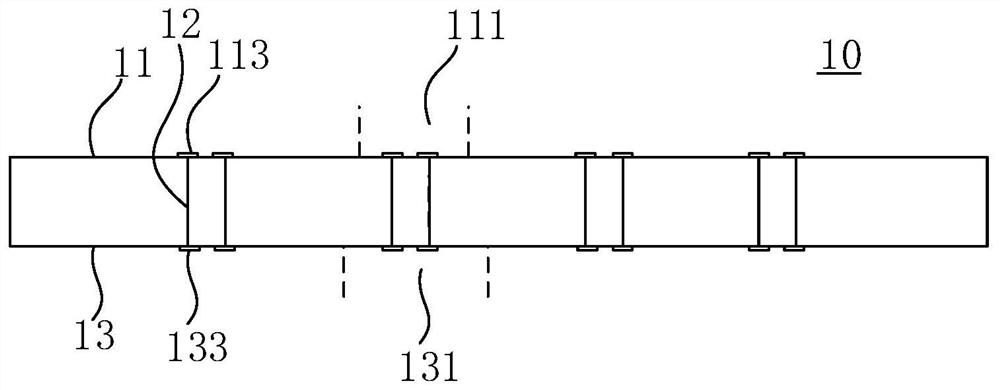
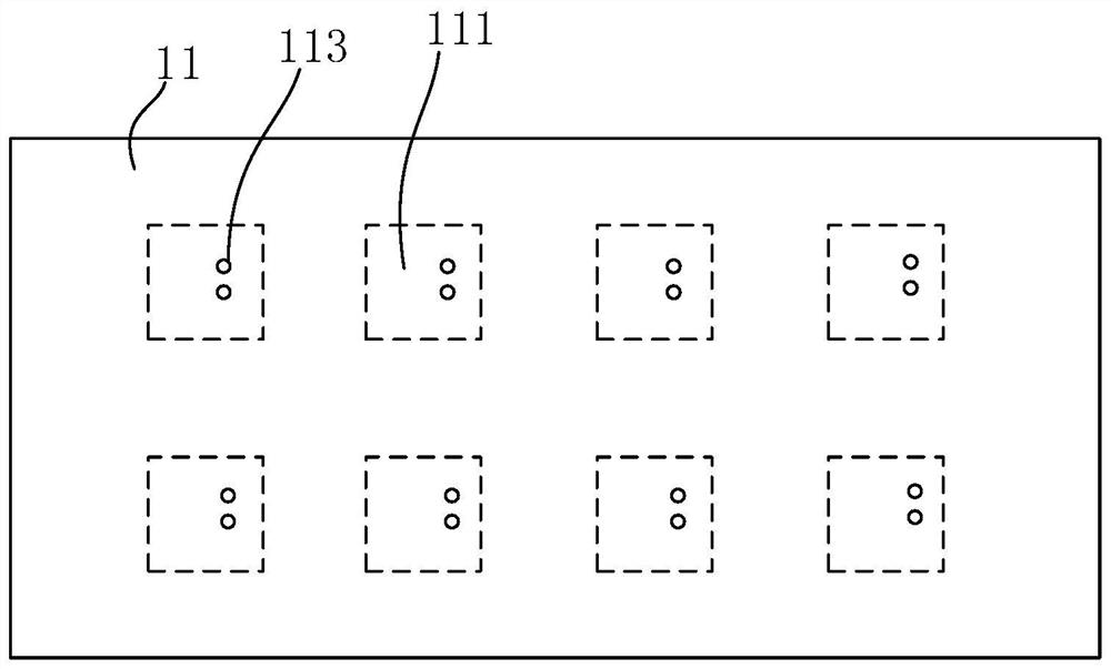
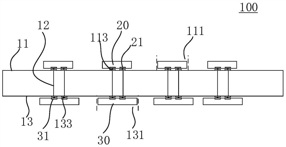
[0030] Please also refer to figure 1 and figure 2 , an embodiment of the present application provides an aging circuit board 10, which is used to perform aging tests on the aging characteristics of chips related to interconnection and the aging characteristics of interconnection functions between chips, for example, for integrated chips with a chiplet architecture. The "chiplets" involved and the interconnection function between the "chiplets" are subjected to burn-in tests.

[0031] It can be understood that since the material environment of the interconnection between...


PUM


Abstract

The invention provides an aging circuit board, an aging test structure and an aging test method, the aging circuit board is provided with a first surface and a second surface, and the first surface and the second surface are oppositely arranged; the first surface is provided with a first connection area, the first connection area is provided with a first connection pad, and the first connection pad is used for connecting a first chip; the second surface is provided with a second connection area, the second connection area is provided with a second connection pad, and the second connection pad is used for connecting a second chip; and the aging circuit board is internally provided with a signal connection structure, and the first connection pad and the second connection pad are in signal connection through the signal connection structure. According to the invention, the signal connection between the first connection pad and the second connection pad is realized through the signal connection structure in the aging circuit board, and the first connection pad and the second connection pad are respectively used for connecting the first chip and the second chip, thereby facilitating the verification of the interconnection function between the first chip and the second chip.

Description

technical field [0001] The present application relates to the field of chip testing, in particular to an aging circuit board, an aging testing structure and an aging testing method. Background technique [0002] The chiplet architecture refers to the disassembly of multiple functions of a traditional SOC (system-on-a-chip, system on a chip) chip, and the development of a variety of small chips that correspond to different functions and can be modularly assembled with each other, for example, The SOC chip is divided into a core circuit chip (Core die) responsible for logic operations and an interface circuit chip (IOdie) responsible for interface circuits. Different types of chiplets can be manufactured using different processes. [0003] At present, the chip testing of the chiplet architecture is usually divided into three stages: the first stage is to conduct wafer-level testing on the chiplets involved in the integrated chip of the chiplet architecture; The small chips i...

Claims


Application Information

Patent Timeline
Patent Type & Authority Applications(China)
IPC IPC(8): H05K1/02H05K1/18G01R31/28
CPCH05K1/02H05K1/18G01R31/2855
Inventor 张亚光
Owner HYGON INFORMATION TECH CO LTD
Why Eureka
Try Eureka