Optoelectronic device

A technology of optoelectronic devices and electrodes, applied in optics, nonlinear optics, instruments, etc., can solve problems such as reducing EAM performance

Pending Publication Date: 2021-10-08
ROCKLEY PHOTONICS INC
View PDF1 Cites 0 Cited by
  • Summary
  • Abstract
  • Description
  • Claims
  • Application Information

AI Technical Summary

Problems solved by technology

In such devices, severe temperature gradients can form across the EAM, which can significantly reduce the performance of the EAM

Method used


Image

  • Optoelectronic device
  • Optoelectronic device
  • Optoelectronic device

Examples


Embodiment Construction

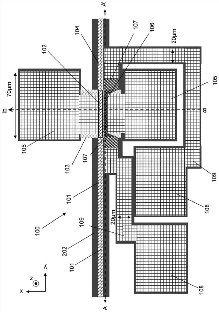
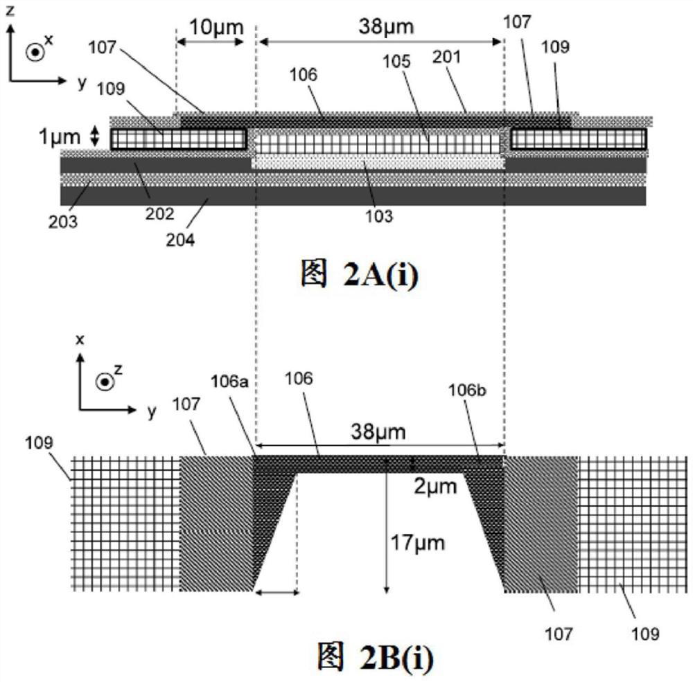
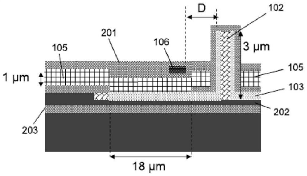
[0090] figure 1 A top view of the optoelectronic device 100 is shown. The input waveguide 101 guides light into a rib waveguide comprising a ridge portion 102 and a slab portion 103 atop a silicon-on-insulator layer 202 . The ridge portion may eg comprise or provide an electroabsorption modulator (EAM) or photodiode structure. Depending on the nature of the ridge portion of the rib waveguide, light may exit the device through the output waveguide 104 . An electrical pad 105, which may be formed from titanium or aluminum, is connected to the rib and plate portions. Typically, the electrodes are formed from 1 μm thick aluminum and may include a 10 nm thick titanium layer between the aluminum and the plate as an electrical barrier. The heater 106 is disposed on top of a part of the flat plate portion 103 . The heater is formed of a substantially elongated metal strip located at a distance of not less than 2 μm from the ridge portion 102 of the rib waveguide. The heaters are ...


PUM

PropertyMeasurementUnit
widthaaaaaaaaaa
heightaaaaaaaaaa
lengthaaaaaaaaaa

Abstract

The invention discloses an optoelectronic device which includes a rib waveguide, the rib waveguide including a ridge portion, incorporating a temperature-sensitive optically active region. The rib waveguide further includes a slab portion, which is positioned adjacent to the ridge portion. The device further includes a heater, which is disposed on top of the slab portion. The part of the heater closest to ridge portion is at least 2 micrometres away from the ridge portion. The device may also have a heater provided in an epitaxial crystalline cladding. In other embodiments the device also includes a bottom cladding layer, and may also include various thermal insulation enhancing cavities.

Description

[0001] This application is a divisional application of an invention patent application with an application date of February 21, 2019, an application number of 201910129798.2, and an invention title of "photoelectric device". technical field [0002] The present invention relates to heaters in optoelectronics, and in particular, to heaters in electroabsorption modulators. Background technique [0003] Optoelectronic devices, especially electroabsorption modulators (EAMs), can be temperature sensitive. For example, the operating wavelength of the EAM can change significantly as the temperature of the device changes. The physical mechanism behind it is that the band-edge wavelength of the material forming the EAM can have temperature dependence. [0004] For example, this temperature dependence may be beneficial when operating in Coarse Wavelength Division Multiplexing (CWDM) mode. However, in this mode of operation, the temperature of the device must be precisely controlled....

Claims


Application Information

Patent Timeline
Patent Type & Authority Applications(China)
IPC IPC(8): G02F1/01G02F1/015G02F1/025
CPCG02F1/0147G02F1/015G02F1/025G02F1/0157G02F2203/21G02F2201/063
Inventor D.Y.伍H.阿贝戴斯尔G.C.拜尔德K.穆思张毅A.J.齐尔基
Owner ROCKLEY PHOTONICS INC
Why Eureka
Try Eureka