Array substrate, preparation method thereof and display device

A technology for array substrates and substrate substrates, applied in semiconductor/solid-state device manufacturing, semiconductor devices, electrical components, etc., can solve problems such as dark spots, avoid dark spots, ensure packaging effects, and improve yields

Pending Publication Date: 2021-10-12
BOE TECH GRP CO LTD +1
View PDF0 Cites 7 Cited by
  • Summary
  • Abstract
  • Description
  • Claims
  • Application Information

AI Technical Summary

Problems solved by technology

However, when the pixel electrodes and isolation columns are formed by an etching process, the isolation columns will react with the etchant to generate metal particles, which is prone to dark spots.

Method used


Image

  • Array substrate, preparation method thereof and display device
  • Array substrate, preparation method thereof and display device
  • Array substrate, preparation method thereof and display device

Examples


Embodiment Construction

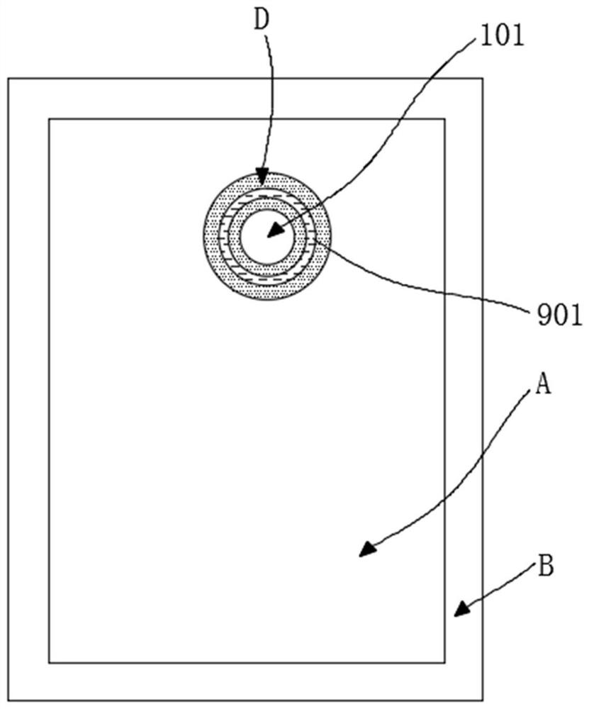
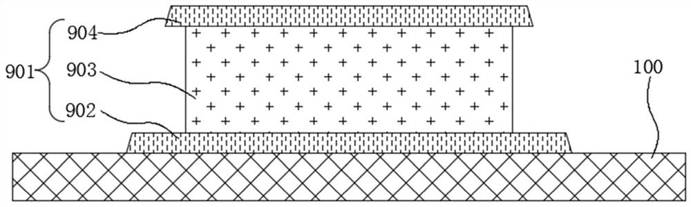
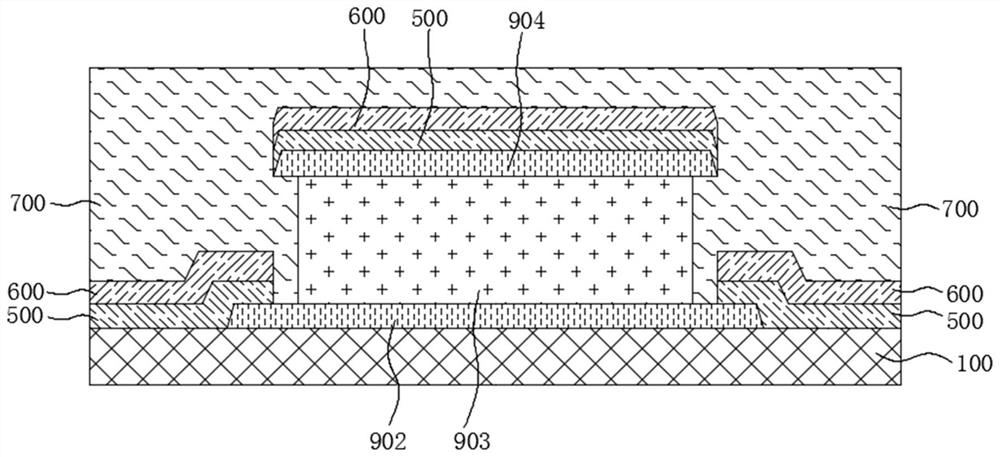
[0071] Example embodiments will now be described more fully with reference to the accompanying drawings. Example embodiments may, however, be embodied in many forms and should not be construed as limited to the examples set forth herein; rather, these embodiments are provided so that this disclosure will be thorough and complete, and will fully convey the concept of example embodiments to those skilled in the art. The described features, structures, or characteristics may be combined in any suitable manner in one or more embodiments. In the following description, numerous specific details are provided in order to give a thorough understanding of embodiments of the present disclosure.

[0072] In the drawings, the thicknesses of regions and layers may be exaggerated for clarity. The same reference numerals in the drawings denote the same or similar structures, and thus their detailed descriptions will be omitted.

[0073] The described features, structures, or characteristic...


PUM


Abstract

The invention provides an array substrate, a preparation method thereof and a display device, and belongs to the technical field of display. The array substrate is provided with a hole opening area and a hole frame area. The preparation method of the array substrate comprises the steps that a source-drain metal layer is formed on one side of a substrate, a first isolation column surrounding a hole opening area is formed in a hole frame area of the source-drain metal layer, and the first isolation column comprises a first metal layer and a second metal layer located on the side, away from the substrate, of the first metal layer; forming a planarization layer at least covering the side surface of each first metal layer; forming a pixel electrode layer; forming a protective layer covering the pixel electrode layer, wherein the protective layer exposes the hole frame area; removing the part, located in the hole frame area, of the planarization layer; partially etching the first metal layer from the side surface to form a third metal layer; removing the protective layer; and sequentially forming an organic light-emitting layer and a common electrode layer. The preparation method of the array substrate can improve the yield of the array substrate.

Description

technical field [0001] The present disclosure relates to the field of display technology, and in particular to an array substrate, a manufacturing method thereof, and a display device. Background technique [0002] With the development of display technology, perforated screens are more and more widely used in mobile phones and other devices. For OLED (Organic Light Emitting Diode) display panels, problems such as water and oxygen intrusion are prone to occur in the perforated area. In order to reduce the risk of water and oxygen intrusion, an isolation column can be formed in the hole frame area through the source and drain metal layer, and the isolation column is used to isolate the organic light-emitting layer and the common electrode layer, thereby blocking the water and oxygen intrusion channel. However, when the pixel electrode and the isolation column are formed through an etching process, the isolation column will react with the etchant to generate metal particles, w...

Claims


Application Information

Patent Timeline
Patent Type & Authority Applications(China)
IPC IPC(8): H01L27/32H01L51/52
CPCH10K59/12H10K50/84H10K59/1201H10K59/124H10K59/122H10K71/621H10K71/00H10K50/844
Inventor 黄炜赟黄耀曾超龙跃承天一
Owner BOE TECH GRP CO LTD
Why Eureka
Try Eureka