Wafer cleaning method and manufacturing method of semiconductor device

A technology of wafer and cleaning fluid, which is applied in semiconductor/solid-state device manufacturing, cleaning methods and appliances, chemical instruments and methods, etc., can solve problems such as device damage failure, device characteristic attenuation, reliability failure, etc., to achieve static electricity suppression, The effect of reducing device failure and improving overall yield

Active Publication Date: 2021-10-15
粤芯半导体技术股份有限公司
View PDF14 Cites 1 Cited by
  • Summary
  • Abstract
  • Description
  • Claims
  • Application Information

AI Technical Summary

Problems solved by technology

Compared with other types of defects (such as particle impurities and organic impurities), the influence caused by static electricity will lead to attenuation of de

Method used


Image

  • Wafer cleaning method and manufacturing method of semiconductor device
  • Wafer cleaning method and manufacturing method of semiconductor device
  • Wafer cleaning method and manufacturing method of semiconductor device

Examples


Embodiment Construction

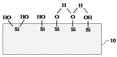
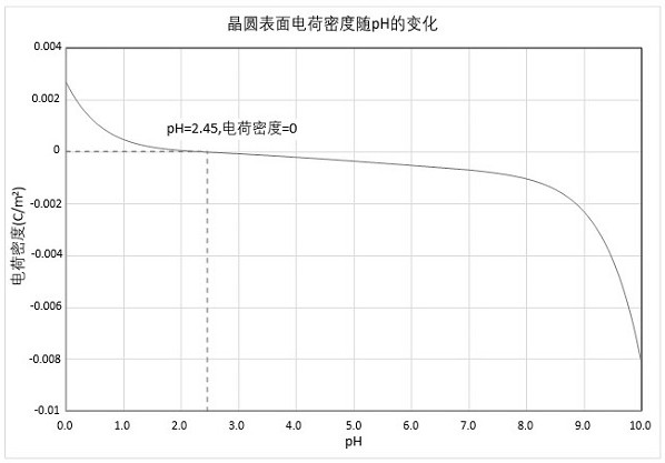
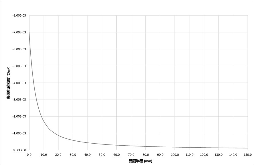
[0053] Since the silicon on the surface of the wafer is very easily oxidized, the surface of the wafer will be covered with a thin layer of silicon dioxide film during the processing of semiconductor devices. When the wafer surface comes into contact with the cleaning solution, the wafer surface becomes charged with a certain amount based on the dissociation / association constant of silica. In cleaning solutions with different electrolyte concentrations and different pHs, the charge amount on the wafer surface is different, and even a point of zero charge (PZC) will appear. The charge generated on the surface of the wafer will not only absorb charged pollutants, but also load the device. In severe cases, it will break down the device like electrostatic discharge, and eventually lead to the scrapping of the product. The mechanism of charge generation on the wafer surface is described below:

[0054] First, see figure 1 , in the process of cleaning the surface of the wafer 10 w...


PUM


Abstract

The invention provides a wafer cleaning method and a manufacturing method of a semiconductor device. The wafer cleaning method comprises the following steps: carrying out protonation treatment on cleaning liquid by adopting a protonation processor; cleaning the surface of the wafer with a protonated cleaning solution, so that the amount of negative charges carried on the surface of the cleaned wafer is smaller than the amount of negative charges carried on the surface of the wafer cleaned with a non-protonated cleaning solution, and the surface of the cleaned wafer is covered with a liquid film of the cleaning solution; and blowing the surface of the wafer by adopting dry gas so as to remove the liquid film from the center to the edge of the surface of the wafer. According to the technical scheme, static electricity on the surface of the wafer can be well restrained, device failure caused by the static electricity is effectively reduced, and then the overall yield of integrated circuit machining is improved.

Description

technical field [0001] The invention relates to the field of integrated circuit manufacturing, in particular to a wafer cleaning method and a semiconductor device manufacturing method. Background technique [0002] For a long time, the development of integrated circuits has followed Moore's Law. According to Moore's Law, the feature size of transistors has continuously evolved from the early micron level to the current nanometer level. As the size of transistors becomes smaller and smaller, the manufacturing process becomes more and more complicated; at the same time, small-sized semiconductor devices are more sensitive to the doping of impurities, especially metal and organic impurities, which will seriously affect the performance characteristics of the device and the reliability of the application. sex. With the increase of the manufacturing process and the strict requirements on the cleanliness of the chip surface, the cleaning process plays an increasingly important rol...

Claims


Application Information

Patent Timeline
IPC IPC(8): H01L21/02B01D61/48B08B11/00
CPCH01L21/02052H01L21/02082H01L21/02057B01D61/48B08B11/00
Inventor 韩瑞津曾辉
Owner 粤芯半导体技术股份有限公司
Why Eureka
Try Eureka