Chip packaging structure integrated with passive element and packaging method

A chip packaging structure and passive component technology, applied in electrical components, electric solid state devices, semiconductor devices, etc., can solve the problems of low integration and large thickness of semiconductor packaging components, and achieve improved heat dissipation performance, high stability, and reliable coupling. high sex effect

Pending Publication Date: 2021-10-29
NAT CENT FOR ADVANCED PACKAGING CO LTD
View PDF1 Cites 0 Cited by
  • Summary
  • Abstract
  • Description
  • Claims
  • Application Information

AI Technical Summary

Problems solved by technology

[0007] Therefore, the technical problem to be solved by the present invention is to solve the problem that the integration degree of the passive elements in the semiconductor package assembly is low, and the thickness of the semiconductor package assembly with multiple passive elements is relatively large.

Method used


Image

  • Chip packaging structure integrated with passive element and packaging method
  • Chip packaging structure integrated with passive element and packaging method
  • Chip packaging structure integrated with passive element and packaging method

Examples


Embodiment 1

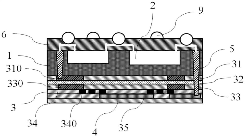
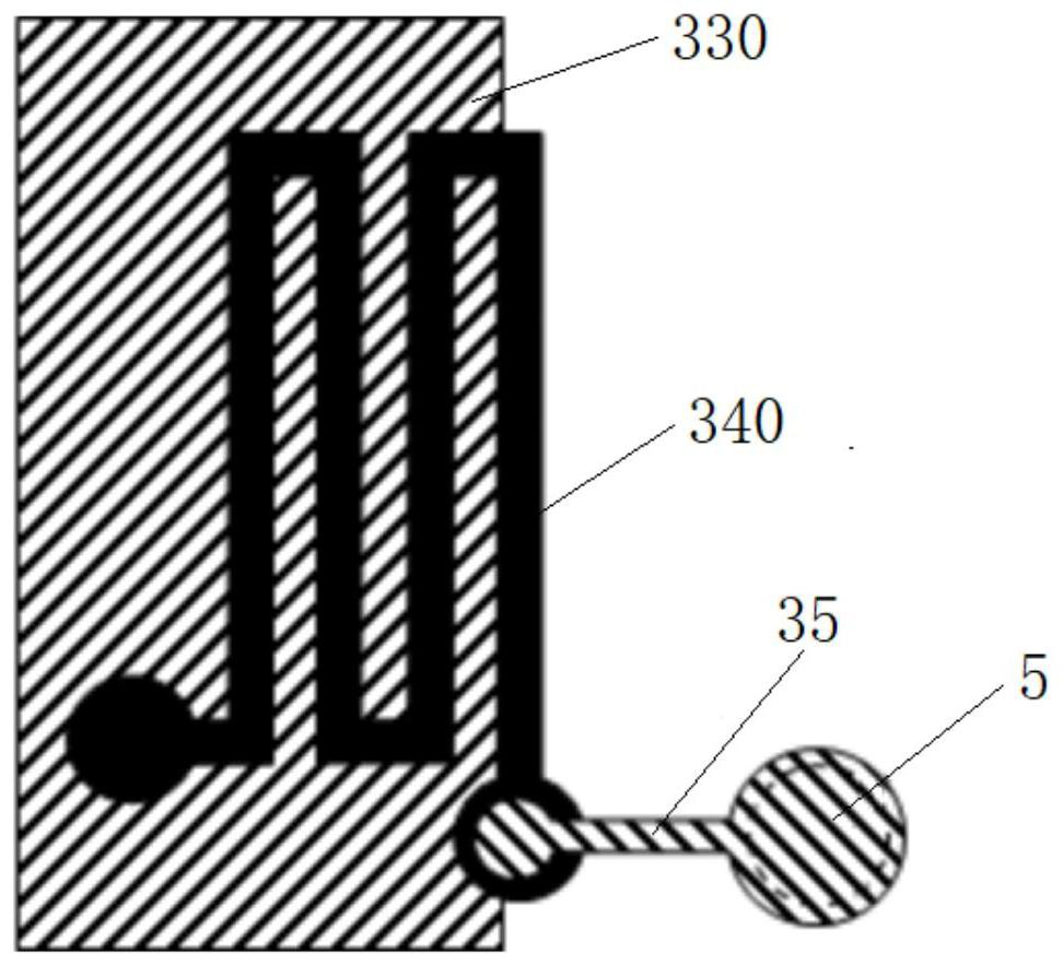
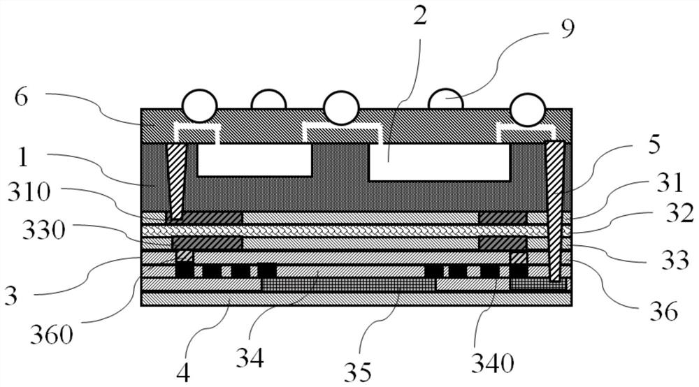
[0037] The embodiment of the present invention improves a chip package structure integrating passive components, such as figure 1 As shown, it includes: a package body 1 with a chip 2 packaged inside; the device surface of the chip 2 is located on the same plane as the first surface of the package body 1; the passive element layer 3 is arranged on the second surface of the package body 1; the first insulating Layer 4 is arranged on the passive element layer 3; the conductive column 5 is arranged in the package body 1, one end of the conductive column 5 is coupled with the passive element layer 3, and the other end is located on the same plane as the first surface of the package body 1; The wiring layer 6 is disposed on the first surface of the package body 1 and coupled with the chip 2 and the conductive pillar 5 . In this embodiment, the device surface of the chip 2 refers to the plane where the pads of the chip 2 are located, and the device surface of the chip 2 is located o...

Embodiment 2

[0052] This embodiment provides a chip packaging method for integrating passive components, such as Figure 5 shown, including the following steps:

[0053] Step S1: providing a substrate, and forming an adhesive layer on the substrate. Such as Figure 6 As shown, in a specific embodiment, the material of the substrate 7 can be glass or ceramics, etc., and the material of the adhesive layer 8 can be thermal release adhesive or UV adhesive film, etc. In a specific embodiment, spray coating, spin coating or film sticking can be used and so on to form the adhesive layer 8 on the substrate 7 .

[0054] Step S2: Paste the device surface of the chip on the pasting layer. Such as Figure 7 As shown, in this embodiment, the device surface of the chip 2 refers to the plane where the pads of the chip 2 are located. In a specific embodiment, there may be one or more chips 2, and the number of chips 2 is determined according to the needs of actual application scenarios.

[0055] Ste...


PUM


Abstract

The invention discloses a chip packaging method integrated with a passive element and a packaging structure formed by the method. The method comprises the steps of forming a bonding layer on a substrate; bonding the device surface of the chip on the bonding layer; forming a packaging body on the bonding layer, and packaging the chip, wherein the thickness of the packaging body is greater than that of the chip; forming a passive element layer on the second surface of the packaging body, wherein the second surface of the packaging body is a surface far away from the device surface of the chip, and the device surface of the chip and the first surface of the packaging body are located on the same plane; forming a first insulating layer on the passive element layer; removing the substrate and the bonding layer, and exposing the device surface of the chip and the first surface of the packaging body; forming a conductive column in the packaging body, wherein one end of the conductive column is coupled with the passive element layer, and the other end of the conductive column and the first surface of the packaging body are located on the same plane; and forming a rewiring layer on the device surface of the chip and the first surface of the packaging body, wherein the rewiring layer is coupled with the chip and the conductive column.

Description

[0001] This application is a divisional application of the application number 2017111841678, the application date is November 23, 2017, and the title is "a chip packaging structure and packaging method for integrated passive components". technical field [0002] The invention relates to the technical field of semiconductor packaging, in particular to a chip packaging structure and packaging method for integrating passive components. Background technique [0003] With the increasing integration of electronic devices, a system-in-package (SIP) has been proposed in the field of semiconductor packaging, which integrates multiple active electronic components with different functions and optional passive devices, and Other devices such as micro-electro-mechanical systems (Micro-Electro-Mechanical System, MEMS) or optical devices are first assembled together to achieve a single standard package with certain functions, thus forming a system or subsystem. [0004] The method widely u...

Claims


Application Information

Patent Timeline
Patent Type & Authority Applications(China)
IPC IPC(8): H01L21/50H01L21/56H01L21/768H01L25/16H01L23/367H01L23/488H01L23/31H01L23/522H01L23/528
CPCH01L23/528H01L25/16H01L21/50H01L23/367H01L21/56H01L21/76877H01L23/488H01L23/31H01L23/5223H01L23/5227H01L23/5228H01L24/02H01L2221/1068H01L2224/0231H01L2224/0237H01L2224/02379H01L2224/18H01L2224/24137H01L2224/12105
Inventor 姚大平
Owner NAT CENT FOR ADVANCED PACKAGING CO LTD
Why Eureka
Try Eureka