A kind of solid crystal method and crystal solid machine

A die-bonding machine and die-bonding technology, which is applied in the fields of electric solid-state devices, semiconductor/solid-state device manufacturing, semiconductor devices, etc. Shortened travel stroke and high efficiency

Active Publication Date: 2021-12-31
SHEN ZHEN TALUER TECH CO LTD
View PDF0 Cites 2 Cited by
  • Summary
  • Abstract
  • Description
  • Claims
  • Application Information

AI Technical Summary

Problems solved by technology

[0002] In the current field of die bonding technology, the biggest difficulty in making large-sized circuit boards is how to realize high-speed wafer transfer. The current mainstream method is swing-arm one-time transfer, that is, the swing-arm suction nozzle picks up the wafer after the blue film Directly transfer to the crystal-bonding point of the circuit board, and the whole process is completed at one time. This method has no problem for small-sized circuit boards, but once the circuit board exceeds 300mm, it seems powerless
There is also a fatal flaw in using a linear motor for one-time transfer to complete the die bonding. The efficiency of large-distance reciprocating movement is too low. The larger the circuit board, the longer the moving distance, and the lower the production efficiency.

Method used


Image

  • A kind of solid crystal method and crystal solid machine
  • A kind of solid crystal method and crystal solid machine
  • A kind of solid crystal method and crystal solid machine

Examples


Embodiment Construction

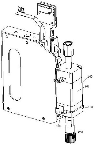
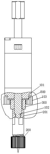
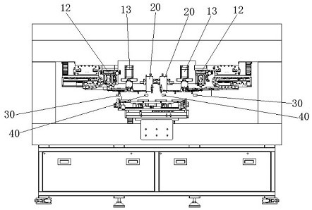
[0029] like figure 1 , 4 , 5, 6, and 7, the present invention discloses a crystal bonding machine, comprising a swing arm mechanism and a linear crystal bonding mechanism, the swing arm mechanism comprising a swing arm 10, a swing arm driving mechanism 13, and the swing arm driving The mechanism 13 is used to drive the swing arm 10 to swing. The swing arm suction nozzle is installed on the swing arm 10; The die-bonding head drive mechanism 21 is used to drive the linear die-bonding head 20 to move; when the swing arm 10 swings to the crystal picking position, push the wafer on the blue film to the swing arm suction nozzle through the thimble 12; When the swing arm 10 swings to the transfer position and the linear die bonding head 20 moves linearly to the transfer position, the die bonding nozzle 200 of the linear die bonding head 20 sucks the wafer on the swing arm suction nozzle; When the linear die bonding head 20 linearly moves to the die bonding position, the die bonding...


PUM


Abstract

The invention provides a crystal bonding method and a crystal bonding machine. The crystal bonding method includes: a crystal extraction step: controlling the swing arm to swing to the crystal extraction position, pushing the wafer on the blue film onto the swing arm suction nozzle through a thimble, Then the swing arm swings to the transfer position; movement control step: control the linear movement of the linear die bonding head to the transfer position; transfer step: when both the swing arm suction nozzle and the linear die bonding head are at the transfer position, control the die bonding The nozzle picks up the wafer on the suction nozzle of the swing arm; the die bonding step: firstly control the linear die bonding head to move to the die bonding position in a straight line, and then control the die bonding nozzle of the linear die bonding head to bond the die to the circuit board. The beneficial effects of the present invention are: the present invention makes a relay on the crystal element at the transfer position through the swing arm suction nozzle and the linear die bonding head, shortens the moving stroke of the linear die bonding head, and adopts the die bonding method and die bonding method of the present invention The crystal machine can not only fix larger circuit boards, but also greatly improve the handling speed of wafers, resulting in higher efficiency.

Description

technical field [0001] The invention relates to the technical field of crystal bonding, in particular to a crystal bonding method and a crystal bonding machine. Background technique [0002] In the current field of die bonding technology, the biggest difficulty in making large-sized circuit boards is how to realize high-speed wafer transfer. The current mainstream method is swing arm transfer, that is, the swing arm suction nozzle picks up the wafer after the blue film Transfer directly to the die-bonding point of the circuit board, and the whole process is completed at one time. This method has no problem for small-sized circuit boards, but once the circuit board exceeds 300mm, it seems powerless. The use of linear motors for one-time transfer to complete the die-bonding also has fatal flaws. The efficiency of long-distance reciprocating movement is too low. The larger the circuit board, the longer the moving distance, and the lower the production efficiency. Contents of ...

Claims


Application Information

Patent Timeline
Patent Type & Authority Patents(China)
IPC IPC(8): H01L21/50H01L21/67H05K3/30H05K13/02H05K13/04
CPCH01L21/50H01L21/67121H01L21/681H01L21/6836H01L21/67242H05K3/30H05K13/02H05K13/04H05K13/0404H01L2221/68304
Inventor 曾逸杨林
Owner SHEN ZHEN TALUER TECH CO LTD
Why Eureka
Try Eureka