Array substrate and display panel

A technology for array substrates and display panels, applied in instruments, nonlinear optics, optics, etc., can solve problems such as error reporting, misidentification, and influence on automatic optical normal detection, so as to improve production efficiency and yield, improve detection efficiency, and reduce errors. The effect of the likelihood of recognition

Active Publication Date: 2022-04-19
HKC CORP LTD
View PDF16 Cites 0 Cited by
  • Summary
  • Abstract
  • Description
  • Claims
  • Application Information

AI Technical Summary

Problems solved by technology

On the basis of COA, placing the spacer on the color filter layer of the array substrate is called POA (PS on Array). The display panel of POA is often provided with a color filter layer in the non-display area, while the array substrate During the production process, the peripheral routing of the non-display area needs to be detected by the peripheral automatic optical inspection AOI (Auto Optical Inspection). Misrecognition, resulting in a large number of error reports, affecting the normal detection of automatic optical detection

Method used


Image

  • Array substrate and display panel
  • Array substrate and display panel
  • Array substrate and display panel

Examples


Embodiment 1

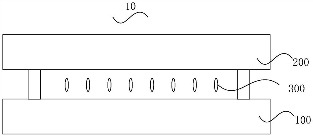
[0031] Such as figure 1 The first embodiment of the present application is shown, which discloses a display panel. The display panel 10 includes an array substrate 100 , a cell substrate 200 and a liquid crystal layer 300 disposed between the two substrates. The array substrate adopts a COA process, that is, the color filter layer is arranged on the array substrate. In order to improve the accuracy rate of the detection of the peripheral wires and reduce misjudgment, the main improvement of the present application lies in the array substrate.

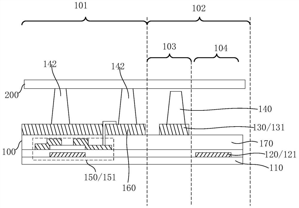
[0032] Such as figure 2 The array substrate 100 in the first embodiment is shown, the array substrate 100 is divided into a display area 101 and a non-display area 102, and the array substrate 100 corresponding to the non-display area 102 includes: a substrate 110, 110 on the peripheral wiring layer 120, the peripheral color resistance layer 130 and a plurality of first spacers 140, the peripheral color resistance layer 130 is arrang...

Embodiment 2

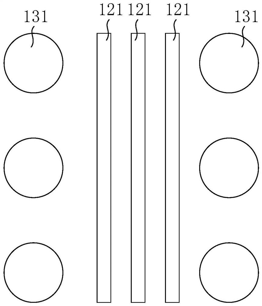
[0042] Such as Image 6 As the second embodiment of the present application, a display panel is disclosed. The display panel includes an array substrate 100 and a box substrate. The array substrate 100 includes: a substrate 110, a 110 on the peripheral wiring layer 120, the peripheral color resistance layer 130 and a plurality of first spacers 140, the peripheral color resistance layer 130 is arranged on the peripheral wiring layer 120, the peripheral color resistance layer 130 includes A plurality of peripheral color resists 131 , the peripheral wiring layer 120 includes a plurality of peripheral wirings 121 , and a plurality of first spacers 140 are correspondingly disposed on the plurality of peripheral color resists 131 . The projection of the peripheral color resist 131 and the peripheral wiring 121 on the substrate 110 does not overlap.

[0043] Specifically, the design of the spacer in the second embodiment is as Image 6 The schematic diagram of the first spacer 140 ...

Embodiment 3

[0051] Such as Figure 8 As shown, as the third embodiment of the present application, the present application also discloses a display panel. The display panel includes: an array substrate 100, a cell substrate and a liquid crystal layer; the cell substrate is arranged opposite to the array substrate 100, and the liquid crystal A layer is disposed between the cell-aligning substrate and the array substrate 100 . The array substrate 100 can be selected from different array substrates 100 in the above-mentioned embodiments. In the selection such as Image 6 On the array substrate 100 in the display panel shown, this embodiment makes certain improvements to the box substrate on the basis of the second embodiment, specifically as follows Figure 8 Shown:

[0052] A black matrix 145 is arranged on the box-matching substrate, and the black matrix 145 is arranged in an area corresponding to the peripheral wiring. The black matrix 145 of the box-matching substrate abuts against th...


PUM


Abstract

The present application discloses an array substrate and a display panel. The array substrate is divided into a display area and a non-display area. The array substrate includes: a substrate and a peripheral track disposed on the substrate corresponding to the non-display area A wire layer, a peripheral color-resist layer and a plurality of first spacers, the peripheral color-resist layer is disposed on the substrate, the peripheral color-resist layer includes a plurality of peripheral color-resistors, and the peripheral wiring layer includes A plurality of peripheral traces, the peripheral color resists and the peripheral traces do not overlap on the projection of the substrate, and the plurality of first spacers are correspondingly arranged on the plurality of peripheral color resists. The present application uses the above solution to reduce the possibility of misidentification during the automatic light detection process.

Description

technical field [0001] The present application relates to the field of display technology, and in particular to an array substrate and a display panel. Background technique [0002] COA (Color Filter on Array) technology is a technology that prepares a color filter layer on an array substrate. The liquid crystal display panel of the existing COA technology combines an array substrate with a color filter layer with a common electrode and a spacer. It is obtained by pairing the opposite substrates, which has the advantages of high aperture ratio and small coupling capacitance. On the basis of COA, placing the spacer on the color filter layer of the array substrate is called POA (PS on Array). The display panel of POA is often provided with a color filter layer in the non-display area, while the array substrate During the production process, the peripheral routing of the non-display area needs to be detected by the peripheral automatic optical inspection AOI (Auto Optical Insp...

Claims


Application Information

Patent Timeline
Patent Type & Authority Patents(China)
IPC IPC(8): G02F1/1362G02F1/1368
CPCG02F1/136222G02F1/136286G02F1/1368
Inventor 张立志郑浩旋
Owner HKC CORP LTD
Why Eureka
Try Eureka