Supercharge Your Innovation With Domain-Expert AI Agents!

Semiconductor packaging device and manufacturing method thereof

A packaging device and semiconductor technology, which is applied in semiconductor/solid-state device manufacturing, semiconductor devices, semiconductor/solid-state device components, etc., can solve the problems of increased warping of rewiring layers, broken conductive lines, and unbearable conductive lines. Achieve the effect of reducing the risk of breaking the conductive line and reducing warpage

Pending Publication Date: 2021-11-05
ADVANCED SEMICON ENG INC
View PDF0 Cites 4 Cited by
  • Summary
  • Abstract
  • Description
  • Claims
  • Application Information

AI Technical Summary

Problems solved by technology

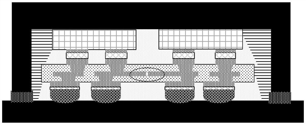
[0002] In the current Fan Out Chip on Substrate (FOCOS) structure, since the thermal expansion coefficient of the dielectric material in the redistribution layer is significantly greater than the thermal expansion coefficient of the metal material of the conductive line, as the number of redistribution layers increases, It is easy to increase the warpage of the entire redistribution layer due to the difference in thermal expansion coefficient of the material, because the conductive lines of the redistribution layer cannot bear the pull of warping, and then produce such as figure 1 The problem of broken conductive lines shown in the dotted line in the middle

Method used


Image

  • Semiconductor packaging device and manufacturing method thereof
  • Semiconductor packaging device and manufacturing method thereof
  • Semiconductor packaging device and manufacturing method thereof

Examples


Embodiment Construction

[0041] The specific implementation manners of the present disclosure will be described below in conjunction with the accompanying drawings and examples. Those skilled in the art can easily understand the technical problems solved by the present disclosure and the technical effects produced through the contents recorded in this specification. It should be understood that the specific embodiments described here are only used to explain related inventions, rather than to limit the invention. In addition, for the convenience of description, only the parts related to the related invention are shown in the drawings.

[0042] It should be noted that the structures, proportions, sizes, etc. shown in the accompanying drawings of the specification are only used to match the content recorded in the specification for the understanding and reading of those skilled in the art, and are not intended to limit the implementation of the present disclosure. There are limited conditions, so it has...


PUM


Abstract

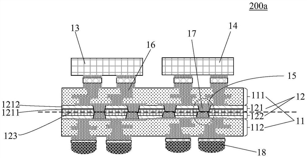
The invention provides a semiconductor packaging device and a manufacturing method thereof. The semiconductor packaging device comprises the components of rewiring layers, a reinforcing layer, a first electronic element and a second electronic element; the rewiring layers comprise an upper rewiring layer and a lower rewiring layer; the reinforcing layer is arranged between the upper rewiring layer and the lower rewiring layer, and the reinforcing layer is provided with a joint interface; and the first electronic element and the second electronic element are arranged on the rewiring layers. According to the semiconductor packaging device and manufacturing method thereof provided by the technical schemes, the reinforcing layer rigidly supports the rewiring layers, and the reinforcing layer can provide pulling force for the rewiring layers to reduce warping of the rewiring layers, so that the risk that a conductive circuit is broken due to warping of the rewiring layers is reduced.

Description

technical field [0001] The present disclosure relates to the technical field of semiconductor packaging, in particular to a semiconductor packaging device and a manufacturing method thereof. Background technique [0002] In the current Fan Out Chip on Substrate (FOCOS) structure, since the thermal expansion coefficient of the dielectric material in the redistribution layer is significantly greater than the thermal expansion coefficient of the metal material of the conductive line, as the number of redistribution layers increases, It is easy to increase the warpage of the entire redistribution layer due to the difference in thermal expansion coefficient of the material, because the conductive lines of the redistribution layer cannot bear the pull of warping, and then produce such as figure 1 The problem of broken conductive lines shown in the middle dotted line. Contents of the invention [0003] In a first aspect, the present disclosure provides a semiconductor packaging ...

Claims


Application Information

Patent Timeline
Patent Type & Authority Applications(China)
IPC IPC(8): H01L23/488H01L21/50
CPCH01L23/488H01L21/50H01L24/02H01L2224/0231H01L2224/02331H01L2224/02379H01L2224/02373
Inventor 张皇贤
Owner ADVANCED SEMICON ENG INC
Features
  • R&D
  • Intellectual Property
  • Life Sciences
  • Materials
  • Tech Scout
  • Unparalleled Data Quality
  • Higher Quality Content
  • 60% Fewer Hallucinations
Learn More