Check patentability & draft patents in minutes with Patsnap Eureka AI!

Storage array circuit, storage array layout and verification method

A storage array and verification method technology, applied in the field of storage array circuits, can solve problems such as consistency verification

Active Publication Date: 2021-11-09
CHANGXIN MEMORY TECH INC
View PDF7 Cites 0 Cited by
  • Summary
  • Abstract
  • Description
  • Claims
  • Application Information

AI Technical Summary

Problems solved by technology

However, the current methods for verifying whether the layout of word lines and bit lines meet the requirements cannot effectively perform layout versus schematic (LVS) consistency verification for word lines and bit lines to verify the layout of word lines and bit lines. The layout meets the requirements

Method used


Image

  • Storage array circuit, storage array layout and verification method
  • Storage array circuit, storage array layout and verification method
  • Storage array circuit, storage array layout and verification method

Examples


Embodiment Construction

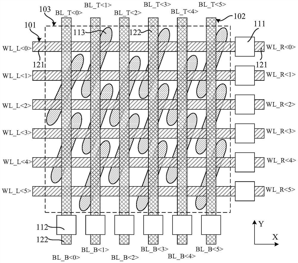
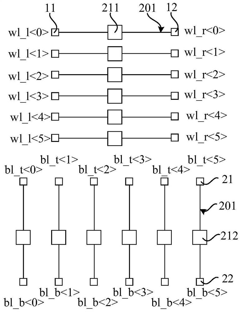
[0014] The storage array includes a plurality of intervalted word lines and a plurality of intervalted bit lines, and each word line is electrically connected to the corresponding word line drive circuit, each bit will be connected with the corresponding sense amplified circuit electricity connect. If the layout of the word line or bit line is an error, it will affect the electrical connection relationship in the storage array. Therefore, the word line layer and the bit line layer in the storage array layout are verified, which is conducive to improving the yield of the storage array.

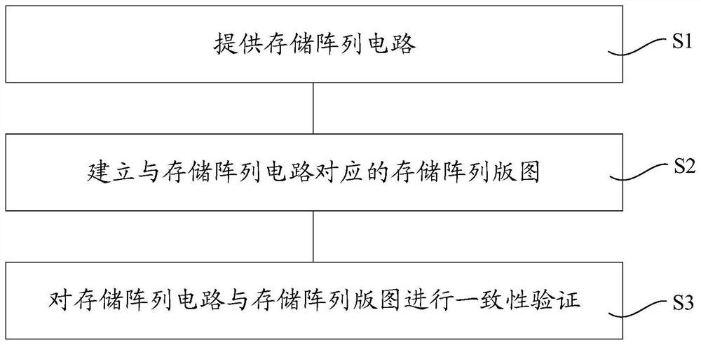
[0015] This application implementation provides a storage array layout that verifies the layout layout of the bit line layer and the word line layer using the storage array layout.

[0016] In order to make the objects, technical solutions, and advantages of the present application, various embodiments of the present application will be described in detail below with reference to the accompanying d...


PUM


Abstract

The embodiment of the invention provides a storage array circuit, a storage array layout and a verification method. The storage array circuit comprises M word lines; M word line breaking nodes, wherein each word line breaking node is used for separating a corresponding word line into a first word line pin and a second word line pin; N bit lines; N bit line breaking nodes, wherein each bit line breaking node is used for separating a corresponding bit line into a first bit line pin and a second bit line pin, wherein the M and the N are positive even numbers. According to the embodiment of the invention, the layout of the word line layer and the bit line layer can be verified.

Description

Technical field [0001] Embodiments of the present application relate to semiconductor technology, and in particular, to a storage array circuit, a storage array layout, and a verification method. Background technique [0002] Dynamic Random Access Memory (DRAM) is a semiconductor memory device that is commonly used in the computer, composed of many duplicated storage units. Each memory cell typically includes a capacitor and a transistor, the gate of the transistor is connected to the word line, and the drain is connected to the bit line. The source is connected to the capacitor, and the voltage signal on the word line can control the opening or closing of the transistor, and then passes through the bit line Read the data information stored in the capacitor or write data information to the capacitor by bit line. [0003] The memory has a plurality of word lines and multiple bit lines, a layout of the word line and bit line meets the requirements, which determines the performance ...

Claims


Application Information

Patent Timeline
Patent Type & Authority Applications(China)
IPC IPC(8): G11C7/12G11C7/18
CPCG11C7/18G11C7/12G11C11/4097G06F30/398G06F30/392Y02D10/00G11C11/4085G11C11/4094
Inventor 汪配焕
Owner CHANGXIN MEMORY TECH INC
Features
  • R&D
  • Intellectual Property
  • Life Sciences
  • Materials
  • Tech Scout
  • Unparalleled Data Quality
  • Higher Quality Content
  • 60% Fewer Hallucinations
Learn More