Non-contact wafer transfer equipment

A non-contact, transfer technology, applied in electrical components, semiconductor/solid-state device manufacturing, circuits, etc., can solve problems such as wafer distortion, chipping, etc., to ensure accuracy and efficiency.

Pending Publication Date: 2021-11-09
苏州桓旭半导体科技有限公司
View PDF0 Cites 2 Cited by
  • Summary
  • Abstract
  • Description
  • Claims
  • Application Information

AI Technical Summary

Problems solved by technology

[0005] Aiming at the problems existing in the prior art, the object of the present invention is to provide a non-contact wafer transfer equipment, which can realize the non-contact firm grasping of the wafer by using the Bernoulli principle, which solves the traditional manual Handling and ordinary negative pressure vacuum suction handling methods may cause wafer distortion or chipping

Method used


Image

  • Non-contact wafer transfer equipment
  • Non-contact wafer transfer equipment
  • Non-contact wafer transfer equipment

Examples


Embodiment 1

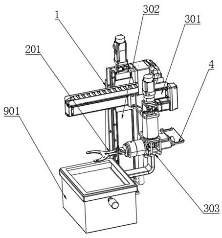
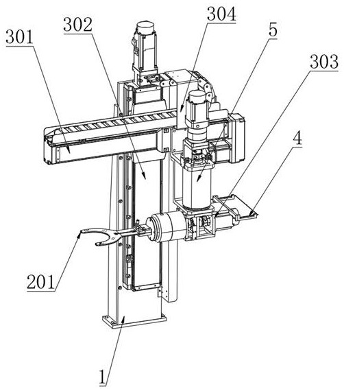
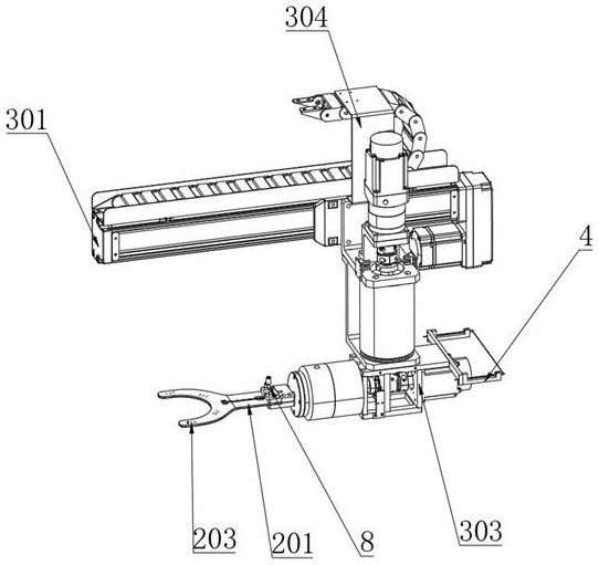
[0036] see Figure 1-10 , a non-contact wafer transfer equipment, including a transfer bracket 1, a suction mechanism 2 is installed on one side of the transfer bracket 1, the suction mechanism 2 includes a Y-shaped gripper 201, and the Y-shaped gripper 201 is installed on the transfer bracket 1. On one side, there are high-pressure air chambers 202 on both sides of the Y-shaped gripper 201, and jet holes 203 are evenly opened on the top of the high-pressure air chamber 202. Inside the jet holes 203, there is a bias flow blocking column 204, and the top side of the bias flow blocking column 204 is installed There is a deflector side plate 205, using the Bernoulli principle, the high-pressure body jet is ejected from the jet hole 203 through the high-pressure air chamber 202, and the jet gas is sprayed laterally around the surface of the Y-shaped claw 201 through the deflection blocking column 204, thereby A cyclone is generated between the surface of the Y-shaped gripper 201 a...


PUM


Abstract

The invention discloses non-contact wafer transfer equipment, and belongs to the field of wafer production. The non-contact wafer transfer equipment comprises a transfer support. A suction mechanism is mounted on one side of the transfer support, is used for sucking and fixing a wafer in a non-contact manner, and comprises a Y-shaped gripper. The Y-shaped gripper is installed on one side of the transfer support, high-pressure air cavities are formed in the two sides of the interior of the Y-shaped gripper, jet flow holes are evenly formed in the tops of the high-pressure air cavities, bias flow blocking columns are arranged in the jet flow holes, and flow guide side plates are installed on one sides of the tops of the bias flow blocking columns. A transfer mechanism is arranged between the Y-shaped gripper and the transfer support. A wafer can be firmly grabbed in a non-contact mode by means of the Bernoulli principle, and the problem that distortion or fragmentation of a wafer can be possibly caused by a traditional manual carrying mode and a common negative pressure vacuum suction carrying mode is solved.

Description

technical field [0001] The invention relates to the field of wafer production, more specifically, to a non-contact wafer transfer device. Background technique [0002] Wafer refers to the silicon wafer used to make silicon semiconductor circuits, and its raw material is silicon. High-purity polycrystalline silicon is dissolved and mixed with silicon crystal seeds, and then slowly pulled out to form cylindrical single crystal silicon. After the silicon ingot is ground, polished, and sliced, it forms a silicon wafer, that is, a wafer. At present, the domestic wafer production lines are mainly 8-inch and 12-inch, and it is necessary to use transfer equipment to move the wafer during detection and etching. [0003] However, traditional manual handling and common negative pressure vacuum suction and handling methods are used for wafer transfer, which may cause distortion or cracking of the wafer. Contents of the invention [0004] 1. technical problem to be solved [0005]...

Claims


Application Information

Patent Timeline
Patent Type & Authority Applications(China)
IPC IPC(8): H01L21/683
CPCH01L21/6838
Inventor 赵学灵彭梓洋
Owner 苏州桓旭半导体科技有限公司
Why Eureka
Try Eureka