Check patentability & draft patents in minutes with Patsnap Eureka AI!

Intelligent conveyor system for semiconductor packaging

An intelligent conveying, semiconductor technology, applied in the direction of conveyor objects, semiconductor/solid-state device manufacturing, transportation and packaging, etc., to achieve cost-saving, simple operation, and space-saving effects

Active Publication Date: 2021-11-23
江苏和睿半导体科技有限公司
View PDF8 Cites 1 Cited by
  • Summary
  • Abstract
  • Description
  • Claims
  • Application Information

AI Technical Summary

Problems solved by technology

[0005] The object of the present invention is to provide a kind of intelligent conveyor system for semiconductor packaging, to solve the problem of the shortcomings of the prior art in the above-mentioned background technology

Method used


Image

  • Intelligent conveyor system for semiconductor packaging
  • Intelligent conveyor system for semiconductor packaging
  • Intelligent conveyor system for semiconductor packaging

Examples


Embodiment Construction

[0031] The technical solutions in the embodiments of the present invention will be clearly and completely described below with reference to the accompanying drawings in the embodiments of the present invention. Obviously, the described embodiments are only a part of the embodiments of the present invention, but not all of the embodiments. Based on the embodiments of the present invention, all other embodiments obtained by those of ordinary skill in the art without creative efforts shall fall within the protection scope of the present invention.

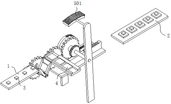
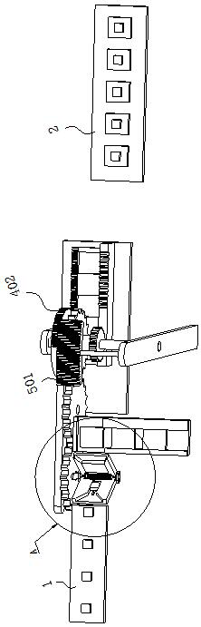
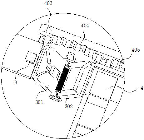
[0032] see Figure 1-9 , an intelligent conveyor system for semiconductor packaging, comprising a feeding and conveying part 1, a transfer processing part and an unloading and conveying part 2; After receiving the substrate 4 and the wafer 3 conveyed by the feeding and conveying unit 1, the transfer processing unit first calibrates the mounting position of the substrate 4 and the wafer 3, and maintains the substrate 4 and the wafer 3 ...


PUM


Abstract

The invention discloses an intelligent conveyor system for semiconductor packaging in the technical field of conveyors. The intelligent conveyor system comprises a feeding conveying part, a transfer treatment part and a discharging conveying part. The feeding conveying part is used for conveying a substrate and a wafer which need to be attached together into the transfer treatment part at the same time. After the transfer treatment part receives the substrate and the wafer conveyed by the feeding conveying part, firstly the attachment positions of the substrate and the wafer are calibrated, the substrate and the wafer are kept at the attachment positions all the time in the transfer process and complete attachment, and the attached substrate and wafer are conveyed to the discharging conveying part when the substrate and the wafer are transferred to the position of the discharging conveying part. According to the intelligent conveyor system, the wafer and the substrate can be stacked and attached in the transfer process, then an attached semiconductor is conveyed to the next production line so as to be packaged, and the production efficiency is improved.

Description

technical field [0001] The invention belongs to the technical field of conveyors, and specifically relates to an intelligent conveyor system for semiconductor packaging. Background technique [0002] Semiconductor packaging is a process in which chips are laid out, fixed and connected on a substrate using technologies such as thin-film microfabrication, and then potted with a plastic insulating medium to form electronic products. The purpose is to protect the chip from damage, ensure the heat dissipation performance of the chip, and realize the power In order to ensure the normal operation of the system, the front side of the chip (that is, the side with the pads on the chip) should be attached to the substrate first, and then wire-bonded, and then packaged. [0003] In the current packaging process, it is necessary to grab the substrate and the wafer from the conveying part respectively, and then stack them for packaging. The program of the grabbing robot has been set durin...

Claims


Application Information

Patent Timeline
Patent Type & Authority Applications(China)
IPC IPC(8): B65G49/06B65G47/22B65G47/84H01L21/677H01L21/67
Inventor 郑石磊郑振军
Owner 江苏和睿半导体科技有限公司
Features
  • R&D
  • Intellectual Property
  • Life Sciences
  • Materials
  • Tech Scout
  • Unparalleled Data Quality
  • Higher Quality Content
  • 60% Fewer Hallucinations
Learn More