
Pixel array, display panel and display device

A display panel and array technology, applied in static indicators, instruments, nonlinear optics, etc., can solve problems such as rough picture quality and vertical crosstalk, avoid low charging efficiency, reduce coupling capacitance, improve rough image quality and vertical crosstalk Effect

Active Publication Date: 2022-07-29
SHENZHEN CHINA STAR OPTOELECTRONICS SEMICON DISPLAY TECH CO LTD
View PDF13 Cites 0 Cited by
  • Summary
  • Abstract
  • Description
  • Claims
  • Application Information

AI Technical Summary

Problems solved by technology

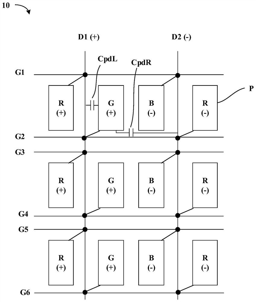
The asymmetry of the coupling capacitance between the pixel and two adjacent data lines will lead to problems such as rough picture quality and vertical crosstalk.

Method used


Image

  • Pixel array, display panel and display device
  • Pixel array, display panel and display device
  • Pixel array, display panel and display device

Examples


Embodiment Construction

[0026] The technical solutions in the embodiments of the present application will be clearly and completely described below with reference to the accompanying drawings in the embodiments of the present application. Obviously, the described embodiments are only a part of the embodiments of the present application, but not all of the embodiments. Based on the embodiments in the present application, all other embodiments obtained by those skilled in the art without creative work fall within the protection scope of the present application.

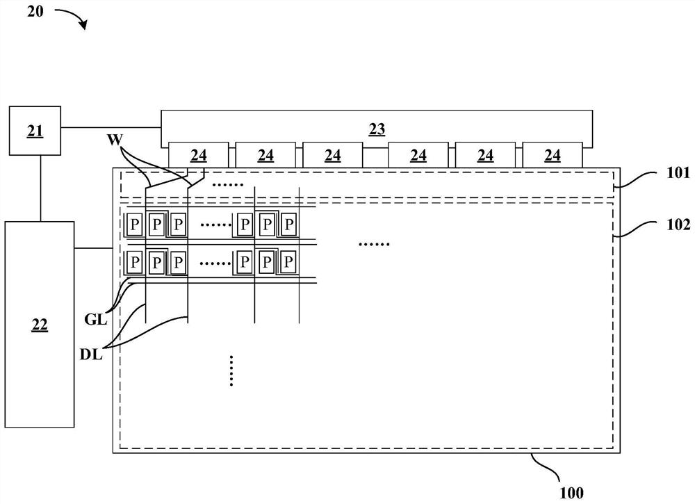
[0027] refer to figure 2 , which shows a schematic diagram of a display device according to an embodiment of the present application. The display device 20 includes a display panel 100 , a controller 21 , a gate driver 22 , a source driver 23 and a plurality of connectors 24 . The controller 21 is connected with the power supply to supply power to the display device 20, and then controls the display device 20 to be turned on or off. The co...


PUM


Abstract

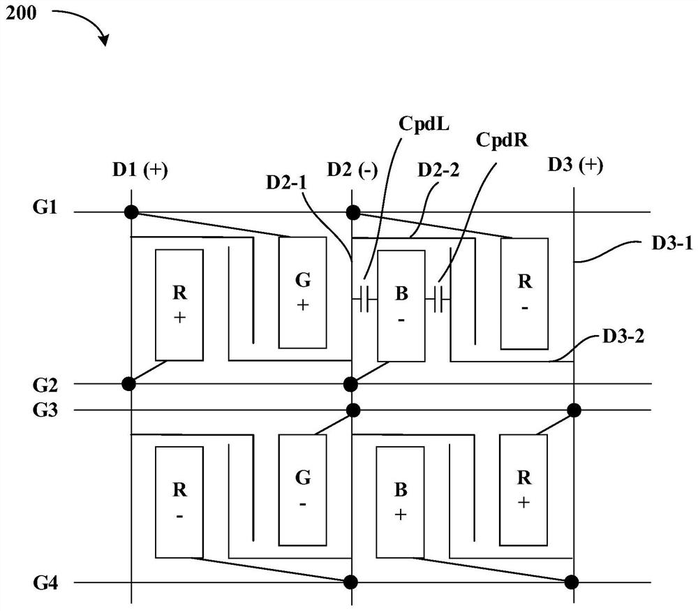
The present application discloses a pixel array, a display panel and a display device. The pixel array includes a first pixel electrode, a first data line and a second data line. The first pixel electrode includes a first side and a second side opposite to the first side. The first data line is electrically connected to the first pixel electrode. The first data line is adjacent to the first side of the first pixel electrode and extends to the second side. The second data line is adjacent to the first data line. At least part of the second data line is disposed between the second side and the first data line. The first data line and the second data line are respectively configured to transmit signals of opposite polarities. In the present application, opposite sides of each pixel are adjacent to two data lines with opposite polarities respectively, thereby improving the problem of vertical crosstalk caused by coupling capacitance and asymmetry on both sides of the pixel.

Description

technical field [0001] The present application relates to the field of display technology, and in particular, to a pixel array, a display panel and a display device. Background technique [0002] With the development of the panel industry, the resolution and refresh rate of the panel have also increased, but it has also resulted in an increase in the number of chip on film (COF) packages disposed in the source driver, which in turn increases the COF sticker. risk of poor bonding and increased costs. Therefore, a data line share (DLS) architecture is proposed. In the DLS architecture, the number of COFs is reduced by half of that of the traditional architecture, thus reducing the risk of poor fit and reducing costs caused by setting up multiple COFs. [0003] figure 1 A schematic diagram of the display panel 10 in the prior art is shown. The display panel 10 includes a plurality of data lines D1-D2, a plurality of gate lines G1-G6, and a plurality of pixels P, wherein the...

Claims


Application Information

Patent Timeline
Patent Type & Authority Patents(China)
IPC IPC(8): G02F1/1343G02F1/1362G02F1/133
CPCG02F1/134309G02F1/136286G02F1/136213G02F1/134318G02F1/13306
Inventor 白一晨龙志娟韦宏权
Owner SHENZHEN CHINA STAR OPTOELECTRONICS SEMICON DISPLAY TECH CO LTD
Learn More