Infrared detector mirror image pixel and infrared detector based on CMOS process

An infrared detector and process technology, applied in the field of infrared detection, can solve the problems of low pixel scale, low yield, and low performance of infrared detectors, and achieve the effects of reducing size, improving detection performance, and increasing radiation absorption

Active Publication Date: 2021-11-30
BEIJING NORTH GAOYE TECH CO LTD
View PDF7 Cites 0 Cited by
  • Summary
  • Abstract
  • Description
  • Claims
  • Application Information

AI Technical Summary

Problems solved by technology

[0012] In order to solve the above-mentioned technical problems or at least partly solve the above-mentioned technical problems, the present disclosure provides an infrared detector mirror image element and an infrared detector. The technical solution solves the problems of low performance, low pixel size and low yield rate of infrared detectors in traditional MEMS technology, and improves the accuracy of detection results

Method used


Image

  • Infrared detector mirror image pixel and infrared detector based on CMOS process
  • Infrared detector mirror image pixel and infrared detector based on CMOS process
  • Infrared detector mirror image pixel and infrared detector based on CMOS process

Examples


Embodiment Construction

[0053] In order to understand the above-mentioned purpose, features and advantages of the present invention more clearly, the solutions of the present invention will be further described below. It should be noted that, in the case of no conflict, the embodiments of the present invention and the features in the embodiments can be combined with each other.

[0054] In the following description, many specific details have been set forth in order to fully understand the present invention, but the present invention can also be implemented in other ways different from those described here; obviously, the embodiments in the description are only some embodiments of the present invention, and Not all examples.

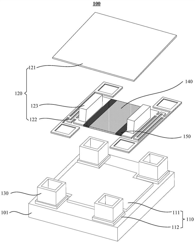
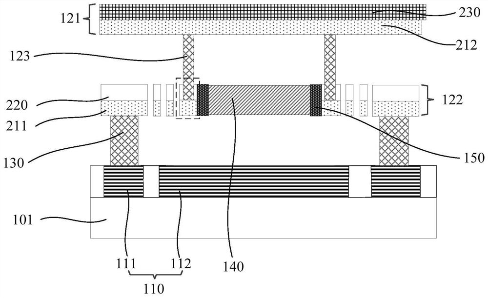
[0055] figure 1 A schematic diagram of a three-dimensional structure of an infrared detector mirror image element based on a CMOS process provided for an embodiment of the present invention, as shown in figure 1 As shown, the infrared detector image element 100 based on the C...


PUM


Abstract

The invention relates to an infrared detector mirror image pixel and an infrared detector based on a CMOS process, the mirror image pixel comprises a CMOS measurement circuit system and a CMOS infrared sensing structure which are both prepared by using the CMOS process, and the CMOS infrared sensing structure is directly prepared on the CMOS measurement circuit system; the CMOS infrared conversion structure comprises a reflecting layer, an infrared conversion structure and a first columnar structure, the reflecting layer comprises a reflecting plate and a supporting base, and the infrared conversion structure is electrically connected with the CMOS measurement circuit system through the first columnar structure and the supporting base; the beam structure is located on the side, close to the CMOS measurement circuit system, of the absorption plate, the CMOS infrared conversion structure further comprises a patterned metal structure arranged corresponding to the beam structure, and at least part of the reflecting plate is located in the orthographic projection of the patterned metal structure. According to the technical scheme, the problems that a traditional MEMS process infrared detector is low in performance, low in pixel scale, low in yield and the like are solved.

Description

technical field [0001] The present disclosure relates to the technical field of infrared detection, and in particular to an infrared detector mirror image element and an infrared detector based on a CMOS process. Background technique [0002] Surveillance market, automotive auxiliary market, home furnishing market, intelligent manufacturing market, and mobile phone applications all have strong demand for uncooled high-performance chips, and have certain requirements for chip performance, performance consistency, and product prices. It is estimated that there is a potential demand of more than 100 million chips every year, but the current process scheme and architecture cannot meet the market demand. [0003] At present, the infrared detector adopts the method of combining the measurement circuit and the infrared sensing structure. The measurement circuit is prepared by CMOS (Complementary Metal-Oxide-Semiconductor, Complementary Metal Oxide Semiconductor) technology, and the...

Claims


Application Information

Patent Timeline
Patent Type & Authority Applications(China)
IPC IPC(8): G01J5/24
CPCG01J5/24G01J2005/0077
Inventor 翟光杰武佩潘辉翟光强
Owner BEIJING NORTH GAOYE TECH CO LTD
Why Eureka
Try Eureka