An etching device for a semiconductor structure

An etching device and semiconductor technology, applied in the fields of semiconductor/solid-state device manufacturing, electrical components, circuits, etc., can solve the particle contamination of semiconductor wafers, the production qualification rate and performance of residual particles in semiconductor wafers cannot be significantly improved, and semiconductor wafers cannot be significantly improved. The circle cannot be completely etched, etc., to achieve the effect of improving the appearance and neatness

Active Publication Date: 2021-12-28
天霖(张家港)电子科技有限公司
View PDF7 Cites 0 Cited by
  • Summary
  • Abstract
  • Description
  • Claims
  • Application Information

AI Technical Summary

Problems solved by technology

[0003] The existing etching technology mainly solves the particle pollution problem of semiconductor wafers. The contaminated particles fall on the untreated semiconductor wafers, and there will be a certain amount of accumulation and accumulation, which can easily cause the contaminated semiconductor wafers to fail. Complete etching, that is to say, when the etched semiconductor wafer is waiting in the equipment, the residual particles on the semiconductor cannot be removed in time, and the residual particles will solidify to a certain extent, which will also cause other subsequent processing. impact, resulting in residual particle production yield and performance on semiconductor wafers that cannot be significantly improved

Method used


Image

  • An etching device for a semiconductor structure
  • An etching device for a semiconductor structure
  • An etching device for a semiconductor structure

Examples


Embodiment Construction

[0033] The following will clearly and completely describe the technical solutions in the embodiments of the present invention with reference to the accompanying drawings in the embodiments of the present invention. Obviously, the described embodiments are only some, not all, embodiments of the present invention. Based on the embodiments of the present invention, all other embodiments obtained by persons of ordinary skill in the art without making creative efforts belong to the protection scope of the present invention.

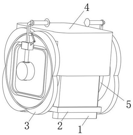
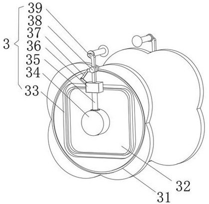
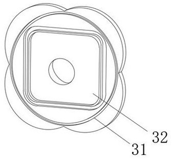
[0034] see Figure 1-7 , the present invention provides a technical solution: an etching device for a semiconductor structure, including a main body 1, the outer surface of the main body 1 is provided with a limiting frame 2, and the outer surface of the main body 1 is fixedly connected to the inner surface of the limiting frame 2, The left end of the limit frame 2 is provided with an etching device 3, and the removal effect of the semiconductor wafer is impro...


PUM


Abstract

The invention discloses an etching device for a semiconductor structure, which comprises a main body, the outer surface of the main body is provided with a limiting frame, and the outer surface of the main body is fixedly connected with the inner surface of the limiting frame, and the left end of the limiting frame is arranged There is an etching device, and the upper surface of the main body is fixedly connected with the bottom end of the metal seat, and the bottom of the inner cavity of the metal seat is provided with a cleaning device. The invention relates to the technical field of semiconductor etching devices. The etching device of the semiconductor structure is equipped with a blocking plate in the middle of the disc, and the rotation of the side stand block will squeeze the blocking plate in the middle of the disc to run, and the disc will operate accordingly, and the disc will be twisted, and the left end of the disc is provided with a swing bar , there is an etching head above the right end of the disk, the disk swings to a certain extent, the bottom of the disk slides along the guide of the placement plate, and the etching head above the right end of the disk also gradually removes the wafer on the semiconductor , to achieve the purpose of comprehensively removing the wafer from multiple angles.

Description

technical field [0001] The invention relates to the technical field of semiconductor etching, in particular to an etching device for semiconductor structures. Background technique [0002] Semiconductors refer to materials whose conductivity is between conductors and insulators at room temperature. Semiconductors are used in integrated circuits, consumer electronics, communication systems, photovoltaic power generation, lighting, high-power power conversion and other fields. For example, diodes are devices made of semiconductors. No matter from the perspective of technology or economic development, the importance of semiconductors is very huge. For most electronic products, etching machines mainly remove wafers without circuit diagrams. Semiconductors cannot be separated from etching. Operating process. [0003] The existing etching technology mainly solves the particle pollution problem of semiconductor wafers. The contaminated particles fall on the untreated semiconductor...

Claims


Application Information

Patent Timeline
Patent Type & Authority Patents(China)
IPC IPC(8): H01L21/67
CPCH01L21/67063
Inventor 吴昌昊黄怡琳田晨阳田英干
Owner 天霖(张家港)电子科技有限公司
Why Eureka
Try Eureka