

Electronic component manufacturing equipment
A technology for electronic components and manufacturing equipment, which is applied in the field of electronic component manufacturing equipment, can solve the problems of reducing equipment sealing requirements, failing to reduce defective rate, increasing chip plastic packaging, etc., so as to avoid overflow of plastic packaging materials and reduce sealing performance Requirements, the effect of improving the yield
- Summary
- Abstract
- Description
- Claims
- Application Information
AI Technical Summary
Problems solved by technology
Method used
Image

Examples
Embodiment 1
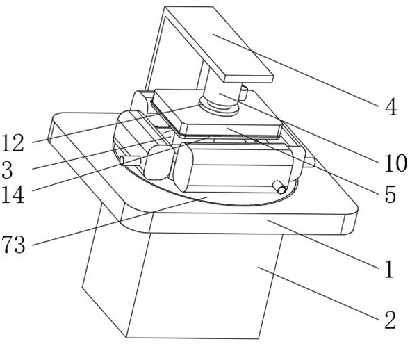
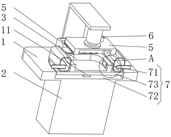
[0039] see Figure 1-5 , the present invention provides a technical solution: a kind of electronic component manufacturing equipment, including an operation table 1, the bottom of the operation table 1 is fixedly connected with a support column 2, the top of the operation table 1 is equipped with a bottom mold 3, and the top of the operation table 1 The support frame 4 is fixedly connected, the bottom of the support frame 4 is equipped with an upper mold 5 through the oil cylinder 10, the top of the upper mold 5 is equipped with an injection pipe 6, the injection pipe 6 runs through the upper mold 5 and extends to the inside of the upper mold 5, and the operation table 1 The above settings are:
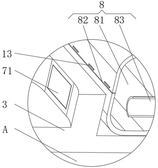
[0040] Heating device 7, the heating device 7 has a heating block 71, the heating block 71 is symmetrically installed on both sides of the inner wall of the bottom mold 3, the top of the console 1 is provided with a rotating groove 72, and the inner wall of the rotating groove 72 is s...
Embodiment 2
[0048] see Figure 1-8 , the present invention provides a technical solution: on the basis of Embodiment 1, a pressing device 9 is arranged above the operating table 1, and the pressing device 9 has a pressing plate 91, and the inner wall of the pressing plate 91 and the upper mold 5 Slidingly connected, both sides of the inner wall of the upper mold 5 are provided with a locking groove 92, and one side of the inner wall of the locking groove 92 is fixedly connected with a locking block 94 through an outwardly pushing spring 93, and the bottom of the locking block 94 is an arc surface. Both sides of the material plate 91 are provided with locking grooves 95 adapted to the locking blocks 94 , and the injection tube 6 runs through the pressure material plate 91 .
[0049] One end of the top of the injection tube 6 is sleeved with an outer tube 15 , the outer tube 15 is slidingly connected with the injection tube 6 , and the bottom of the outer tube 15 is fixedly connected with t...
PUM
 Abstract
Description
Claims
Application Information